

Automatic dynamic range control circuit
a dynamic range control and circuit technology, applied in the direction of volume compression/expansion, volume compression/expansion having semiconductor devices, waveguide type devices, etc., can solve the problem of exhibiting a transient response characterized by both attack and decay time, and the signal-to-noise ratio will naturally be lower
- Summary
- Abstract
- Description
- Claims
- Application Information
AI Technical Summary
Benefits of technology
Problems solved by technology
Method used
Image

Examples
first embodiment
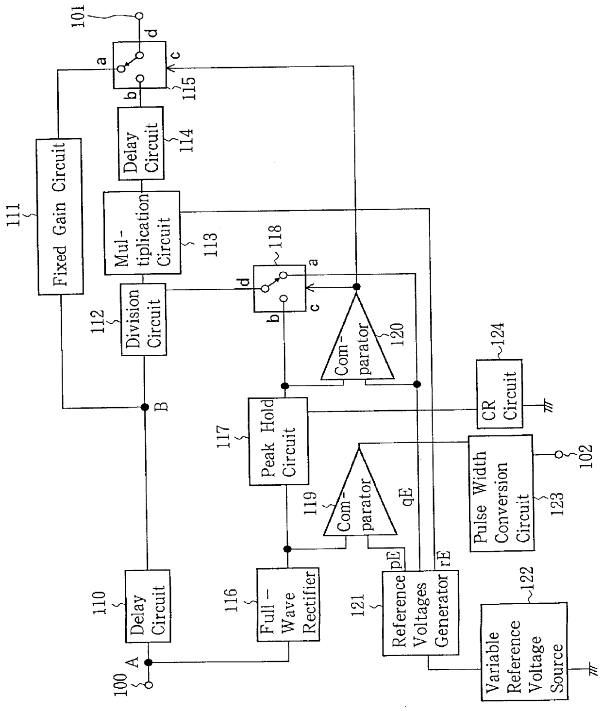
FIG. 1 is a block diagram of an automatic dynamic range control circuit according to this invention. This circuit comprises input terminal 100, output terminal 101, output terminal 102 for a signal causing a warning lamp to flash, delay circuits 110 and 114, fixed gain circuit 111, division circuit 112, multiplication circuit 113, switching circuit 115, full-wave rectifying circuit 116, peak hold circuit 117, switching circuit 118, comparators 119 and 120, reference voltages generator 121, variable reference voltage source 122, pulse width conversion circuit 123, and CR circuit 124 for controlling the decay time of peak hold circuit 117.
A description will now be given of the signal flow in this first embodiment and of the functions of its various circuits.
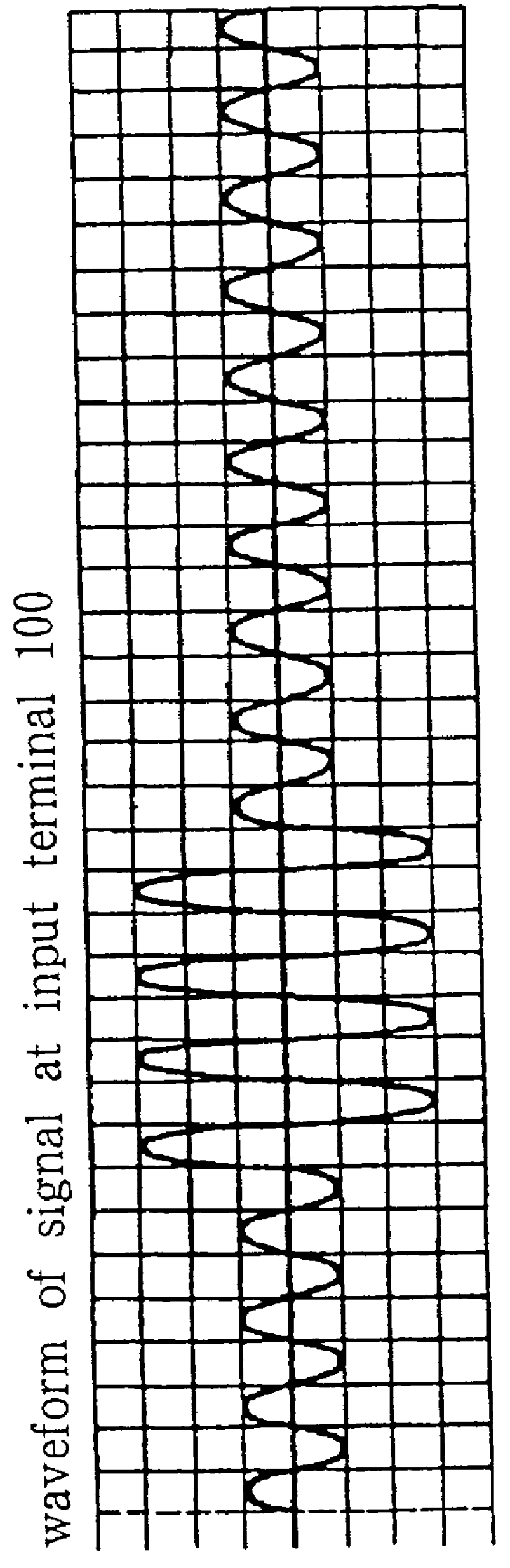
A signal f(t) input from input terminal 100 is first of all split into two branches at point A, with one branch being delayed by delay circuit 110 having a delay of .gamma., giving a signal K1f(t-.gamma.), where K1 is the amplifica...
second embodiment
FIG. 5 shows this invention. This embodiment comprises input terminal 200, output terminal 201, output terminal 202 for a signal causing a warning lamp to flash, delay circuits 210 and 214, fixed gain circuit 211, division circuits 212 and 230, switching circuits 215 and 218, full-wave rectifying circuit 216, peak hold circuit 217, comparators 219 and 220, reference voltages generator 221, variable reference voltage source 222, pulse width conversion circuit 223, and CR circuit 224 for controlling the decay time of peak hold circuit 217.
A description will now be given of the signal flow in this second embodiment depicted in FIG. 5, and of the functions of its various circuits.
A signal f(t) input from input terminal 200 is first of all split into two branches at point A, with one branch being delayed by delay circuit 210 having a delay of .gamma., giving a signal K1f(t-.gamma.), where K1 is the amplification factor (or attenuation) of delay circuit 210. The output of delay circuit 21...
third embodiment
This third embodiment is configured so that when the output (control) signal of comparator 320 is low, the signal obtained as the output of division circuit 330 is:
It follows that the output of multiplication circuit 313 is:
and that the signal formed at terminal b of switching circuit 315 is:
where .zeta. is the delay of multiplication circuit 313.
Next, if the output of comparator 320 is high, i.e., if
the output of division circuit 330 will be:
where .zeta. is the delay of division circuit 330. The signal obtained at terminal b of switching circuit 315 is therefore:
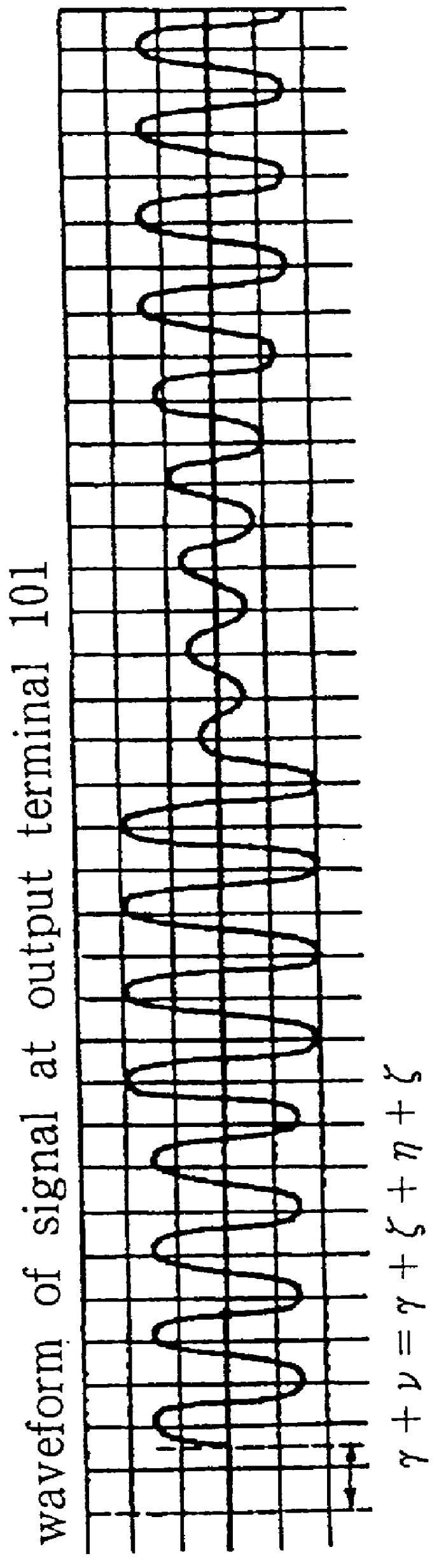
In this embodiment, the state of terminal a and of terminal b immediately before switching circuit 315 switches can be described respectively by Equation (9) and Equation (10) above. It follows that the values of the two equations must be equal in order for the waveform present at output terminal 301 to be smooth and continuous immediately after the circuit has switched. Setting these conditions, we get:
It may be noted that...
PUM
 Abstract
Description
Claims
Application Information