
Using NO or N2O treatment to generate different oxide thicknesses in one oxidation step for single poly non-volatile memory

a non-volatile memory and oxidation step technology, applied in the direction of semiconductor devices, basic electric elements, electrical appliances, etc., can solve the problems of nitrogen implantation not being a good idea, pollution and degradation of oxide films, and affecting the quality of tunnel oxid

Inactive Publication Date: 2000-08-29
TAIWAN SEMICON MFG CO LTD
View PDF11 Cites 31 Cited by
  • Summary
  • Abstract
  • Description
  • Claims
  • Application Information

AI Technical Summary

Benefits of technology

Another object of the present invention is to provide an effective and very manufacturable method of forming a thicker tunnel oxide in a memory portion of an integrated circuit device and a thinner transistor oxide in a periphery portion of an integrated circuit device using a single oxidation step.
A further object of the invention is to prevent photoresist damage to the tunnel oxide when forming transistor oxide films in the periphery of a memory circuit.

Problems solved by technology

This composite tunnel oxide degrades the quality of the tunnel oxide.
Removal of the photoresist mask may cause pollution and degradation of the oxide film.
However, the nitrogen implantation is not a good idea for tunnel oxide because the implant will damage the substrate.
No shielding layer is used over the tunnel oxide or the peripheral oxide which also would degrade quality.

Method used


Image

  • Using NO or N2O treatment to generate different oxide thicknesses in one oxidation step for single poly non-volatile memory
  • Using NO or N2O treatment to generate different oxide thicknesses in one oxidation step for single poly non-volatile memory
  • Using NO or N2O treatment to generate different oxide thicknesses in one oxidation step for single poly non-volatile memory

Examples


Embodiment Construction

The following example is given to show the important features of the invention and to aid in the understanding thereof. Variations may be made by one skilled in the art without departing from the spirit and scope of the invention.

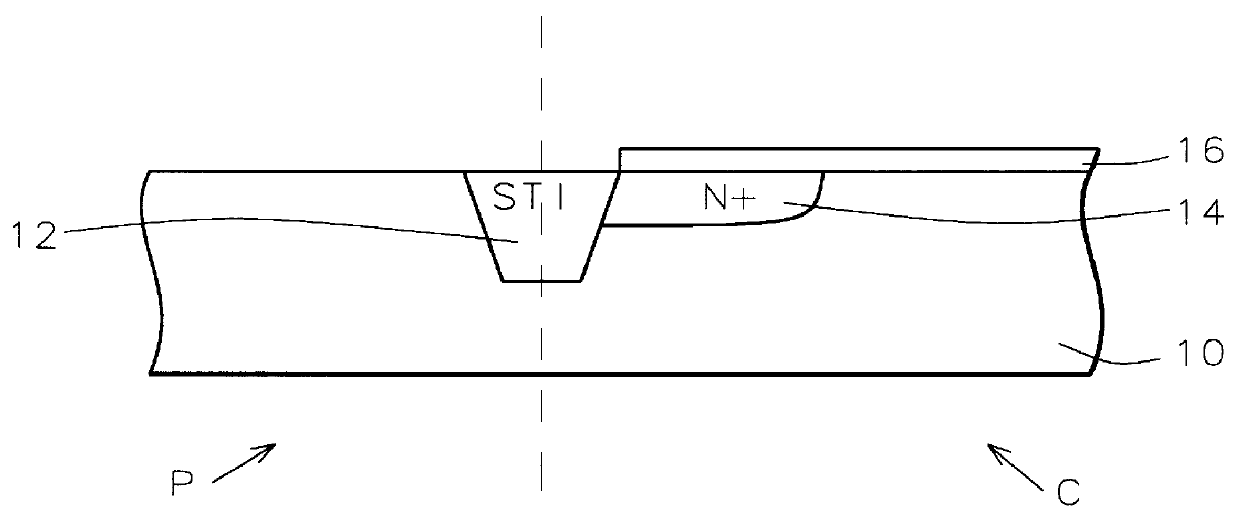
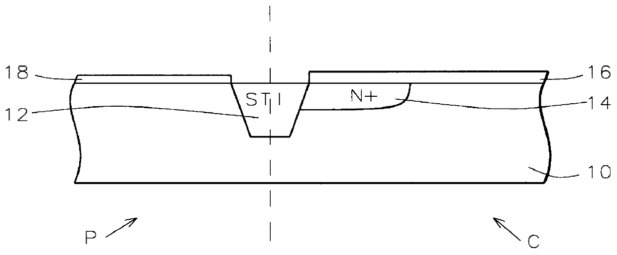
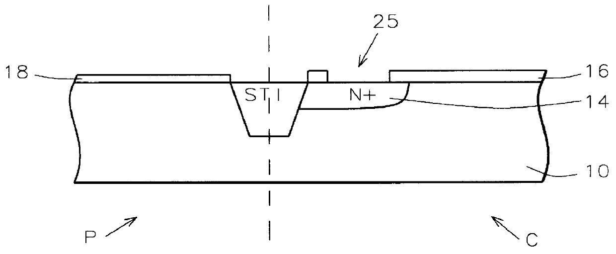
The process of the invention has been implemented and tested on a control wafer. First, the rapid thermal process (RTP) of the invention was performed to form the nitrogen-containing silicon oxide layer (18 in FIG. 4). The RTP was performed at 900.degree. C. for durations from 20 to 60 seconds, as shown in Table 1. Next, the tunneling window was opened and the furnace thermal oxidation was performed. Thicknesses in Angstroms of the first oxide layer in the periphery area (P), the resulting oxide layer 28 in the periphery area (P) and the tunnel oxide layer 26 in the cell area (C) are shown in Table 1.

Table 1 shows the experimental data for the process of the invention using NO treatment. N.sub.2 O data ware similar, but slightly poorer. Both treatment optio...


PUM


Abstract

A new method of using a NO or N2O treatment on a first area on a wafer in order to form a thinner oxide film in the first area and a thicker oxide film in a second area on a wafer using a single oxidation step is achieved. A semiconductor substrate of a silicon wafer is provided wherein a first area is separated from a second area by an isolation region. The silicon substrate in the second area is treated with NO or N2O whereby a high-nitrogen silicon oxide layer is formed on the surface of semiconductor substrate in the second area. A tunnel window is defined in the first area and the oxide layer within the tunnel window is removed. The silicon wafer is oxidized whereby a tunnel oxide layer forms within the tunnel window and whereby a gate oxide layer is formed overlying the high-nitrogen silicon oxide layer in the second area. The tunnel oxide layer has a greater thickness than the combined thickness of the gate oxide layer and the high-nitrogen silicon oxide layer. A conducting layer is deposited and patterned overlying the tunnel oxide layer and the gate oxide layer and fabrication of the integrated circuit device is completed.

Description

(1) Field of the InventionThe invention relates to a method of fabricating embedded memory devices, and more particularly, to a method of fabricating embedded memory devices in which one oxidation step can provide a thicker tunnel oxide and a thinner periphery transistor oxide simultaneously in the fabrication of integrated circuits.(2) Description of the Prior ArtIn the deep sub-micron process of single-poly non-volatile memory, the oxide thickness of the periphery transistors must be smaller than that of the tunnel oxide. In a conventional process, a second oxidation is performed to thicken the tunnel oxide. This composite tunnel oxide degrades the quality of the tunnel oxide. In another conventional process, a gate oxide is grown, then removed in one area. A second area is shielded by photoresist while the first area is reoxidized. Removal of the photoresist mask may cause pollution and degradation of the oxide film.U.S. Pat. No. 5,600,164 to Ajika et al shows a memory device hav...

Claims


Application Information

Patent Timeline
Patent Type & Authority Patents(United States)
IPC IPC(8): H01L21/02H01L21/336
CPCH01L29/66825Y10S438/981
Inventor YU, MO-CHIUNCHU, WEN-TINGJANG, SYUN-MIN
Owner TAIWAN SEMICON MFG CO LTD
Learn More