Ball limiting metalization process for interconnection

a metalization process and ball limiting technology, applied in the direction of improving the adhesion of the insulating substrate, printed circuit aspects, printed circuit manufacturing, etc., can solve the problems of insulator damage quite easily, insulator damage could occur quite easily, and the bottom cu remains unreacted

Inactive Publication Date: 2000-08-29
IBM CORP
View PDF6 Cites 119 Cited by
  • Summary
  • Abstract
  • Description
  • Claims
  • Application Information

AI Technical Summary

Problems solved by technology

Since the solder interconnection lies on top of the thin insulator layer on the chip surface and the joint is often subjected to mechanical and thermal stressing, the damage to the insulator could occur due to a localization of film stress within the joint.
Specifically, the insulator damage could occur quite readily if the edges of the Cr and the Cu layers coincide.
However, due to the presence of an intervening top Cr--Cu phased layer, the bottom Cu remains unreacted.
This pro

Method used


Image

  • Ball limiting metalization process for interconnection
  • Ball limiting metalization process for interconnection
  • Ball limiting metalization process for interconnection

Examples


Embodiment Construction

This invention is related a method of forming a solder joint by a two masking step BLM process which can be adjusted to provide any level of edge separation between the various layer edges to reduce edge stress.

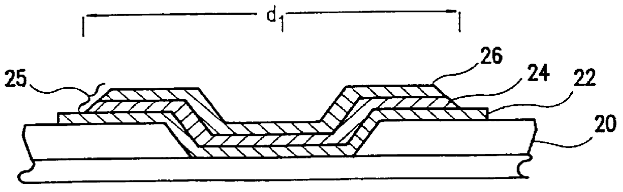
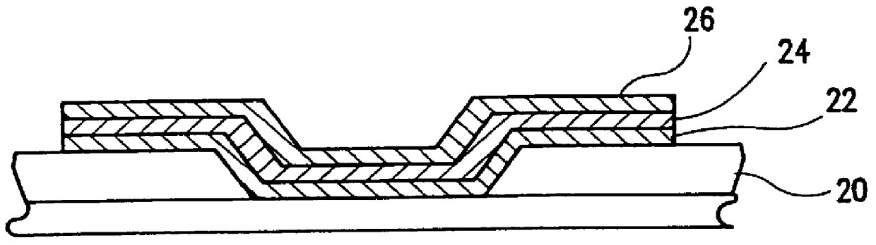
Referring now to the drawings, and more particularly to FIG. 2, there is shown a supporting substrate 20 to which a semiconductor chip is to be electrically and mechanically connected by a solder joint. Three blanket layers, including a solder non-wettable adhesion layer 22, a phased layer 24, and a solder wettable layer 26, are sequentially deposited onto substrate surface 20. Any number of well known deposition methods may be used to accomplish this, such as, for example, physical vapor deposition or sputtering. The non-wettable layer 22 may be, for example, chromium (Cr), titanium (Ti), Zirconium (Zr), molybdenum (Mo), tantalum (Ta), or any other metal or alloy which will adhere to the surface of the supporting substrate 20 or semiconductor chip (not shown). The wettable l...


PUM


Abstract

A two-step masking process is disclosed for forming a ball limiting metallurgy (BLM) pad structure for a solder joint interconnection used between a support substrate and a semiconductor chip. A solder non-wettable layer and a solder wettable layer are deposited on the surface of a support substrate or semiconductor chip which are to be connected. A phased transition layer is deposited between the wettable and non-wettable layers. A thin photo-resist mask defines an area of the solder wettable and phased layers which are etched to form a raised, wettable frustum cone portion. A second mask is deposited on the surface of the support substrate or semiconductor chip, and has an opening concentrically positioned about the frustum cone. Solder is deposited in the opening and covers the frustum cone and the area about its periphery. When solidified, the solder, acting as a mask, is used to sub-etch the underlying solder non-wettable layer thereby defining the BLM pad. When reflowed, the solder beads away from the surface of the solder non-wettable layer to form a ball which securely adheres about the frustum cone.

Description

1. Field of the InventionThe present invention generally relates to a method for adhering a semiconductor chip to a supporting substrate and, more particularly, to a solder ball limiting metallurgy (BLM) process for improving the integrity of solder joint interconnections between a substrate and a chip.2. Description of the Prior ArtSolder ball connections have been proven very successful for electrically connecting a semiconductor chip to a supporting substrate. Since the substrate surface is solder non-wettable, Pb / Sn (lead / tin) solder does not bond to the substrate surface directly. Hence, an intermediate pad structure must normally be used between the two surfaces to facilitate adhesion. U.S. Pat. No. 5,027,188 to Owada et al. shows an example of this type of solder joint wherein an adhesion pad, commonly known as ball limiting metallurgy (BLM), is interposed between a chip and, for example, an Sn / Pb alloy solder ball.The solder ball fabrication could be done by use of either a ...

Claims


Application Information

Patent Timeline
IPC IPC(8): H01L21/02H01L21/48H01L21/60H05K1/11H05K3/34H05K3/38
CPCH01L21/4853H05K3/3452H01L24/11H01L2224/0401H01L2224/03912H01L2224/05564H01L2224/1147H01L2224/13006H01L2224/13099H01L2924/01013H01L2924/01022H01L2924/01027H01L2924/01029H01L2924/0104H01L2924/01042H01L2924/01046H01L2924/01073H01L2924/01078H01L2924/01079H01L2924/01082H05K1/112H05K3/3457H05K3/388H05K2201/09472H05K2201/09509H05K2201/2081H05K2203/043H01L2924/01005H01L2924/01006H01L2924/01024H01L2924/01033H01L2924/014H01L2924/00013H01L2224/29099H01L2924/351H01L2224/0558H01L2224/05556H01L2224/05664H01L2224/05155H01L2224/05655H01L2224/05164H01L2224/05169H01L2224/05147H01L2224/05166H01L2224/05171H01L2224/05157H01L2224/05669H01L2224/05181H01L2224/05647H01L2224/0518H01L2224/0517H01L24/13H01L24/05H01L24/03H01L2924/00H01L2924/00012H01L2924/00014H01L2924/013
Inventor AGARWALA, BIRENDRA NATH
Owner IBM CORP
Why Eureka
Try Eureka