
Optical coupler and a method of producing it

a technology of optical couplers and optical light guides, applied in the field of optical couplers, can solve the problems of increasing the cost, not being able to put the method to practical use, and wasting a lot of time in the optical axis alignment of every optical waveguide elemen

Inactive Publication Date: 2000-08-29
KYOCERA CORP
View PDF3 Cites 57 Cited by
  • Summary
  • Abstract
  • Description
  • Claims
  • Application Information

AI Technical Summary

Benefits of technology

said optical element is mounted on said plural parts at said portion. With this arrangement, any stresses and strains in the substrate after jointing are moderated to effectively control and prevent fluctuations in the positioning accuracy of the optical connection.
characterized in that the portion for mounting the optical element of said first substrate is provided with plural trapezoidal protrusions provided with solder bumps, and that melting temperatures of said solder bumps vary from protrusions to protrusions. Thus bonding between the substrate and the optical element can be effected stepwise by using the self-alignment effect of the solders; hence positioning can be made with high precision.
Further, preferably, the heights of said protrusions are varied from each other. As a result, during bonding of the substrate and the optical element, the optical element stepwise comes to contact with plural protrusions through solders. This further improves the positioning accuracy.
According to the present invention, with a construction wherein a base substrate, of which coefficient of thermal expansion is substantially identical to that of an optical element, is bonded onto the back of a substrate, and the substrate is provided with a portion for mounting an optical element, that is divided into plural parts, or with a construction wherein a portion for mounting an optical element on one principal face of a substrate is provided with plural trapezoidal protrusions on which solder bumps are formed, and the melting temperatures of the solders differ from protrusion to protrusion, the present invention has excellent effects that bonding of the substrate and the optical element to be mounted on the substrate can be done with high precision of positioning through simple steps using the self-alignment effect of solder, and that even if the substrate and the optical element differ in coefficient of thermal expansion, stresses and strains that are generated in the substrate during bonding and after bonding are moderated to effectively suppress and prevent fluctuations in the positioning accuracy of the optical connection, and in turn, to produce products of high reliability at lower cost.
Further, when an optical coupler, in which the portion for mounting an optical element of the substrate is divided into parts, is to be produced, through a step of providing a first mask for V-groove formation on one principal face of the substrate of Si, a step of providing a second mask for forming the portion for mounting an optical element that is to be divided on the other principal face of the substrate, a step of giving anisotropic etching to the two principal faces, next a step of bonding the substrate onto the base substrate, and a step of removing the first mask, the present invention has excellent effects that the substrate can be directly divided, without damaging the base substrate, to form the portion for mounting an optical element, and that the divided portion for mounting an optical element can be bonded onto the base substrate without disturbing the formation of the divided portion.

Problems solved by technology

However, optical connection between an integrated optical waveguide element and an optical fiber requires precise alignment, that took much time and was a cause of an increased cost in the past.
This method, however, requires transmission of light beam through the light waveguide and subsequent adjustment, and in turn, much time for optical axis alignment of every optical waveguide element, and is costly.
However, as precision and reproducibility of positioning by the self-alignment effect of solder are not sufficient, this method has not been put to practical use yet.
Another problem of this method is that, when the optical waveguide element and the substrate differ in coefficient of thermal expansion, the solder joints will be subjected to large stresses due to high temperature at the time of solder reflow and due to changes in environmental temperature at the time of use; as a result, the joints tend to fail at a higher rate, and pose the problem of reliability.
However, the application of this method to optical connection between an optical waveguide element, that uses a material having electrooptic effect or piezoelectric effect, such as LN, and optical fiber poses a problem.
As the size of the optical waveguide element is large in general, and the optical waveguide element and the substrate of Si, etc. differ greatly in coefficient of thermal expansion, a large strain tends to be generated in the substrate during bonding or after bonding, that in turn prevents achievement of the desired alignment accuracy or generates cracks in joints of the substrate during the service.

Method used


Image

  • Optical coupler and a method of producing it
  • Optical coupler and a method of producing it
  • Optical coupler and a method of producing it

Examples


Embodiment Construction

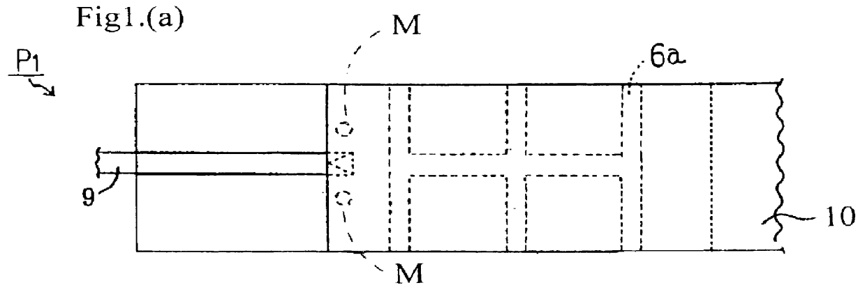
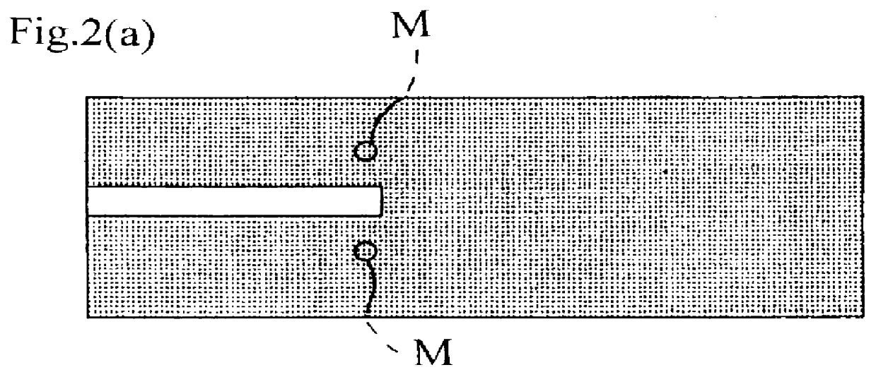
Optical couplers of embodiments of the present invention will be described with reference to FIG. 1 through FIG. 6. FIG. 1 (a) is a plan view of an optical coupler P1, and FIG. 1 (b) is a side view of it. FIG. 2 through FIG. 4 show production steps of the optical coupler P1, and in each set of diagrams, (a) is a plan view of the optical coupler P1, and (b) is a side view of it. FIG. 5 is a perspective view of an optical coupler P2 of an embodiment, and FIGS. 6 (a) through (c) are side views illustrating the method of bonding a substrate and a optical element of the optical coupler P2 through the use of the self-alignment effect of solder.

In FIG. 1, 1 denotes a substrate, and in one of its principal faces is formed a V-groove 4 for mounting an optical fiber. 3 is a thin film of Cr / Au, that is provided on a surface of the block 1a to be bonded with a base substrate 8. The thin film 3 has a good wettability with solder. 4 is the V-groove for mounting an optical fiber. 6 is a gap that i...


PUM


Abstract

An optical coupler wherein on one principal face of an Si single crystal substrate are formed, by etching, grooves for mounting optical fibers and a portion for mounting an optical element that is divided into plural parts, a base substrate, of which coefficient of thermal expansion is substantially identical to that of the optical element, is bonded onto the other principal face of the substrate, and the optical element is mounted on the portion for mounting an optical element.

Description

The present invention relates to an optical coupler, that is used in optical communication systems based on optical fiber, optical information processing systems such as optical computers, etc., and a method of producing thereof.PRIOR ARTFIG. 7 is a perspective view showing a conventional optical coupler P wherein an LN optical waveguide element 34, that is made of a single crystal of lithium niobate (LN: LiNbO3), is mounted as an optical element. In the LN optical waveguide element 34, for example, an optical waveguide 35 is formed on the surface of an LN substrate, and the refractive index of the optical waveguide 35 is higher than that of LN, or in addition to it, an electric field, magnetic field, sound or the like is applied to the optical waveguide 35 to modulate the optical output strength, the direction of deflection of light, the polarization of light or the like.This optical coupler P is structured by mounting and fixing a substrate for mounting an optical element 31, the ...

Claims


Application Information

Patent Timeline
IPC IPC(8): G02B6/30G02B6/42
CPCG02B6/30G02B6/4232
Inventor KISHIDA, YUJIKOMEDA, RYUJIKUBA, YUTAKAMATSUBARA, TAKAHIRO
Owner KYOCERA CORP
Features
  • Generate Ideas
  • Intellectual Property
  • Life Sciences
  • Materials
  • Tech Scout
  • Unparalleled Data Quality
  • Higher Quality Content
  • 60% Fewer Hallucinations
Learn More