Matrix substrate, liquid-crystal device incorporating the matrix substrate, and display device incorporating the liquid-crystal device

a liquid crystal device and matrix substrate technology, applied in the direction of identification means, instruments, optics, etc., can solve the problems of increasing manufacturing costs, increasing manufacturing equipment costs, and increasing electrical severe characteristics

Inactive Publication Date: 2000-10-03
CANON KK
View PDF23 Cites 92 Cited by
  • Summary
  • Abstract
  • Description
  • Claims
  • Application Information

AI Technical Summary

Problems solved by technology

With increase in the screen size, however, manufacturing equipment will become more expensive and electrically severe characteristics will be demanded for driving the large screen.
Therefore, with increase in the screen size, the manufacturing cost will rapidly increase in proportion to the square to the cube of the size.
However, since polycrystalline Si is inferior to monocrystalline Si, in order to realize high-definition televisions of a higher resolution level than in the NTSC standards or displays of the XGA (extended Graphics Array) or SXGA (Super extended Graphics Array) class in the resolution standards of computer, a plurality of separate shift registers must be provided.
However, when the signal line driving circuit is constructed of the plurality of separate shift registers, the fact is that this arrangement is not completely free of occurrence and instability of the noise called the ghost discussed above.

Method used


Image

  • Matrix substrate, liquid-crystal device incorporating the matrix substrate, and display device incorporating the liquid-crystal device
  • Matrix substrate, liquid-crystal device incorporating the matrix substrate, and display device incorporating the liquid-crystal device
  • Matrix substrate, liquid-crystal device incorporating the matrix substrate, and display device incorporating the liquid-crystal device

Examples


first embodiment

[First Embodiment]

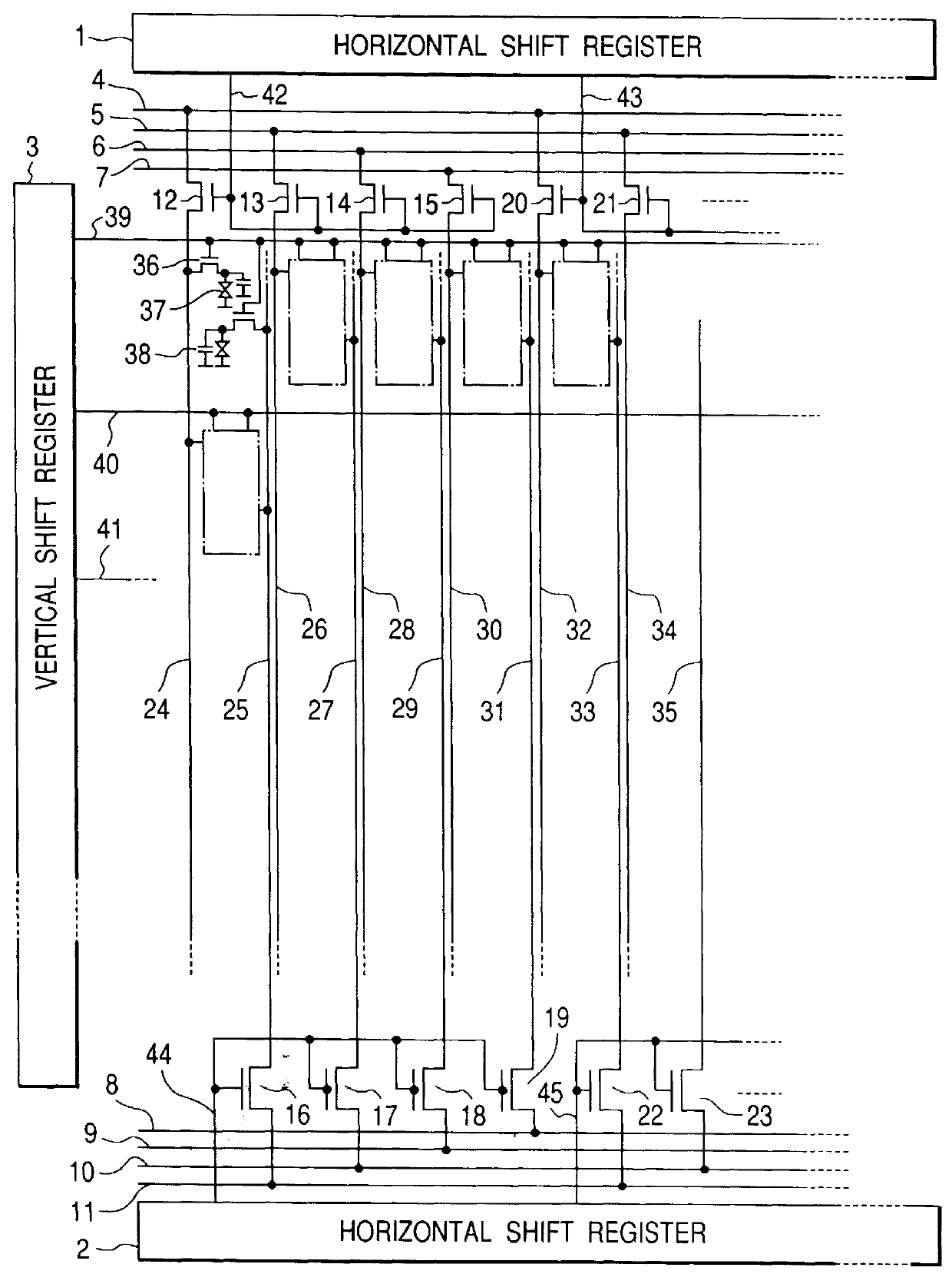
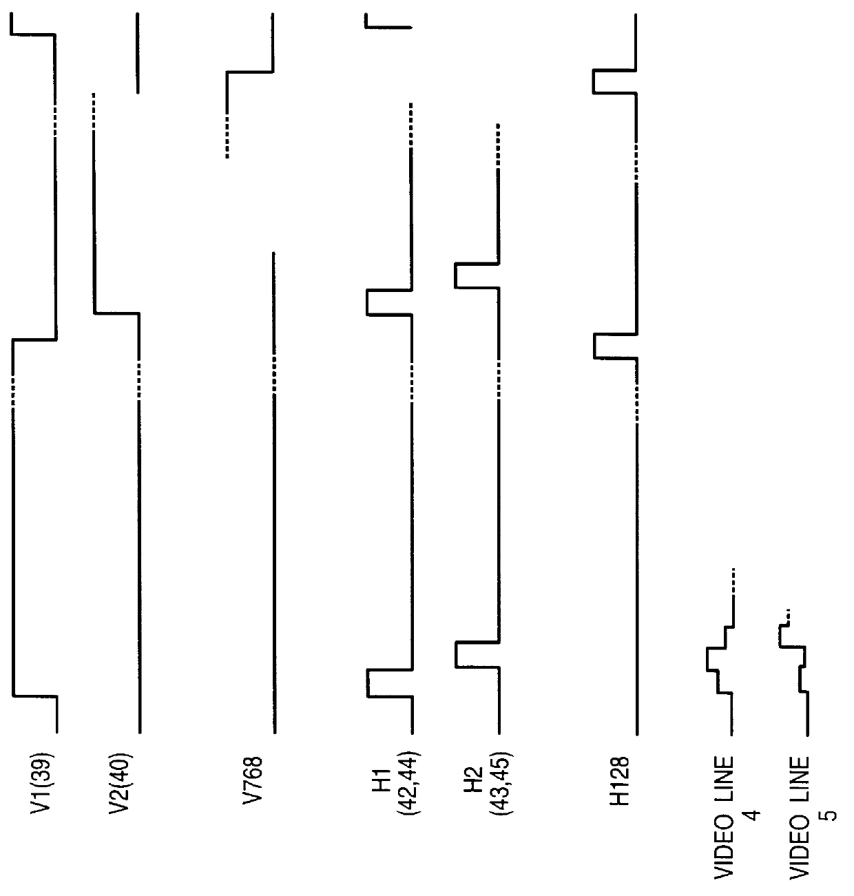
The first embodiment of the present invention will be described. In FIG. 8, reference numerals 401, 402 designate the horizontal shift registers (horizontal driving circuit), 403 the vertical shift register (vertical driving circuit), 404 to 407 the video lines for video signals, 408 to 415 . . . the sampling transistors for sampling the video signals in accordance with the scanning pulses from the horizontal shift registers, 416 to 423 the signal lines to which the video signals are supplied through the sampling transistors 408 to 415 . . . , and 424 to 433 the switching transistors of pixel section each including the liquid crystal interposed between the common electrode and the pixel electrode and the additional capacitor for temporarily holding pixel charge. Numerals 434, 435 denote the driving lines for output from the vertical shift register 403, and 436 to 439 the output lines from the horizontal shift registers.

The basic operation of this example is the sam...

second embodiment

[Second Embodiment]

FIG. 9 is a circuit diagram of the liquid-crystal panel of the present example. In FIG. 9, 101, 102 designate the horizontal shift registers, 103 the vertical shift register, 104 to 107 the video lines for video signals, 108 to 115 . . . the sampling transistors for sampling the video signals in accordance with the scanning pulses from the horizontal shift registers, 116 to 119 . . . the signal lines to which the video signals are supplied through the sampling transistors 108 to 115 . . . , and 120 to 123 . . . the switching transistors of pixel section each including the liquid crystal 130 interposed between the common electrode and the pixel electrode and the additional capacitor 131 for temporarily holding the pixel charge. Numerals 124, 125 denote the driving lines for output from the vertical shift register 103, each of which is divided into two horizontal scanning lines to be connected to the switching transistors 120 to 123 . . . of pixel section. Further, ...

embodiment 3

[Embodiment 3]

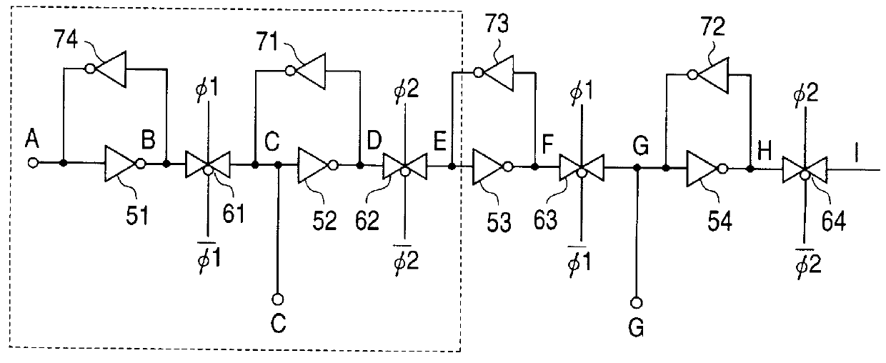
The basic configuration is the same as in Embodiment 2 shown in FIG. 9, but the configuration of the horizontal shift register circuit is different. FIG. 14 is a diagram of the shift register circuit. Numeral 500 denotes the dynamic shift register shown in FIGS. 11A and 11B, and booster circuits 501, 502, 503, . . . a reconnected to outputs of the respective inverters. The output from the shift register indicated by numeral 126 in FIG. 9 is outputted from B. Each sampling transistor 108 to 115 is illustrated as one MOS transistor in FIG. 9, but, without having to be limited particularly to this example, it is needless to mention that the sampling transistors may be transfer gates of CMOS transistor or the like. When the transfer gates of CMOS transistor are used, the output A from the booster circuit 501, 502, 503, . . . is also used and is connected to the gate of pMOS transistor. Numeral 504 represents a clock buffer of clock .phi.1 (.phi.2), which drives long wires ...


PUM

PropertyMeasurementUnit
frequencyaaaaaaaaaa
gate capacitanceaaaaaaaaaa
voltage dropaaaaaaaaaa

Abstract

A matrix substrate comprises a plurality of pixel electrodes arrayed in a matrix pattern, a plurality of switching elements connected to the pixel electrodes, a plurality of signal lines for supplying video signals to the plurality of switching elements, a plurality of scanning lines for supplying scanning signals to the plurality of switching elements, a horizontal driving circuit for supplying the video signals to the plurality of signal lines, and a vertical driving circuit for supplying the scanning signals to the plurality of scanning lines, wherein the horizontal driving circuit is comprised of a dynamic type circuit and the vertical driving circuit is comprised of a static type circuit.

Description

1. Field of the InventionThe present invention relates to a matrix substrate, a liquid-crystal device for displaying images and letters by use of the matrix substrate and liquid crystal, and a display device incorporating the liquid-crystal device. More particularly, the invention concerns a liquid-crystal device and a display device characterized by a horizontal driving circuit and a vertical driving circuit for driving liquid-crystal elements.2. Related Background ArtAs the world moves into the multimedia age nowadays, devices for communications by image information are increasing their importance. Among others, liquid-crystal display devices are drawing attention because of their small thicknesses and low consumption power and have grown to one of basic industries, as comparable to semiconductors. The liquid-crystal display devices are now used mainly in 10-inch size notebook personal computers. It is to be expected that the liquid-crystal display devices of larger screen sizes w...

Claims


Application Information

Patent Timeline
Patent Type & Authority Patents(United States)
IPC IPC(8): G09G3/36G02F1/133G02F1/1335G02F1/13357G02F1/1343G02F1/1368G09F9/35
CPCG09G3/3648G09G3/3677G09G3/3688G09G2300/0823G09G2330/021G09G2310/0251G09G2310/0283G09G2310/0297G09G2320/041G09G2310/0205G09G3/3614G09G3/3233G09G2310/0286
Inventor ICHIKAWA, TAKESHIMIYAWAKI, MAMORUKUREMATSU, KATSUMIKOYAMA, OSAMU
Owner CANON KK
Why Eureka
Try Eureka