Advanced trench sidewall oxide for shallow trench technology

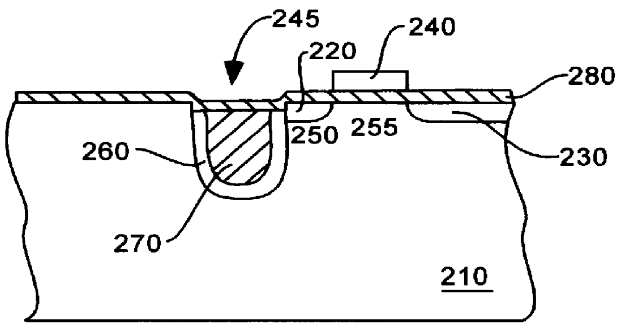
a technology of trench sidewall oxide and trench, which is applied in the direction of semiconductor/solid-state device manufacturing, basic electric elements, electric devices, etc., can solve the problems of parasitic capacitance, the formation of the "bird's beak" or the top corner 190 of the trench, and the limited number of transistors that can be built on the silicon substra

Inactive Publication Date: 2000-11-28
INTEL CORP
View PDF15 Cites 53 Cited by
  • Summary
  • Abstract
  • Description
  • Claims
  • Application Information

AI Technical Summary

Problems solved by technology

In general, the number of transistors that can be built on a silicon substrate is limited only by the size of the transistors and available surface area on the substrate.
There are several problems, however, that result from use of the trench isolation technology described briefly above.
One such problem is the formation of the "bird's beak" or sharp top corners 190 of the trench.
Sharp top corners 190 of the trench may carry stronger electric fields (e-fields) and cause problems later when forming active regions on either side of the trench.
For example, once a transistor is formed and is functioning, the sharp top corners 190 create a high e-field and the thin gate oxide layer 180 may be subject to failure causing undesirable parasitic capacitances and leakage voltages that degrade device performances.
As a result, the isolation technique described above is limited to fabricating devices that use a thin gate oxide layer of greater than 32 .ANG..
Sharp top corners can also cause a prob...

Method used


Image

  • Advanced trench sidewall oxide for shallow trench technology
  • Advanced trench sidewall oxide for shallow trench technology
  • Advanced trench sidewall oxide for shallow trench technology

Examples


Embodiment Construction

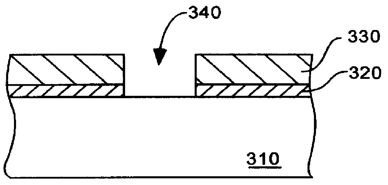
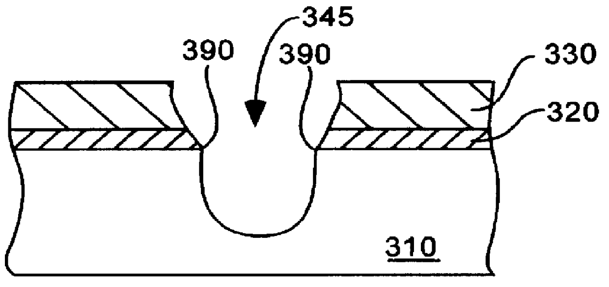
An improved method for forming N.sub.2 O nitrided-oxide trench sidewalls that reduce boron outdiffusion and decrease stress is disclosed. In the following description, numerous specific details are set forth such as specific materials, process parameters, dimensions, etc. in order to provide a thorough understanding of the present invention. It will be obvious, however, to one skilled in the art that these specific details need not be employed to practice the present invention. In other instances, well-known materials or methods have not been described in detail in order to avoid unnecessarily obscuring the present invention.

Embodiments of the present invention provide a trench isolation structure and a method for making that structure that will reduce dopant out diffusion and also allow substantially uniform deposition of thin gate oxides. In the manufacture of semiconductor devices embodiments of the present invention are employed to form a barrier between the trench and an active...


PUM


Abstract

A method of forming an isolation structure in a semiconductor substrate is described. A trench is first etched into a semiconductor substrate. The trench is subjected to a nitrogen-oxide gas ambient and is annealed to form a silicon-oxynitride surface along the trench sidewalls. A first oxide layer is then formed within the trench. The first oxide layer is subjected to a nitridation step and is annealed to form an oxy-nitride surface on the first oxide layer and a silicon-oxynitride interface between the first oxide layer and the semiconductor substrate. A second oxide layer is then deposited over the oxy-nitride surface of the first oxide layer. The method and isolation structure of the present invention reduce dopant outdiffusion, reduce trench stresses, allow more uniform growth of thin gate oxides, and permit the use of thinner gate oxides.

Description

1. Field of the InventionThe present invention relates generally to the field of semiconductor processing, and more particularly, to a trench isolation process.2. Description of the Related ArtAs the demand for cheaper, faster, lower power consuming microprocessors increases, so must the device packing density of the integrated circuit (IC). All aspects of the IC must be scaled down to fully minimize the dimensions of the circuit. In addition to minimizing transistor dimensions, one must minimize the dimensions of the field regions (or isolation regions) which serve to physically and electrically isolate one semiconductor device from an adjacent semiconductor device on a semiconductor substrate, so that each device can operate independently of the other.In general, the number of transistors that can be built on a silicon substrate is limited only by the size of the transistors and available surface area on the substrate. Transistors can only be built in active regions of a silicon s...

Claims


Application Information

Patent Timeline
IPC IPC(8): H01L21/762H01L21/70
CPCH01L21/76235
Inventor ARGHAVANI, REZACHAU, ROBERT SARCOT, BINNY
Owner INTEL CORP
Why Eureka
Try Eureka