Process to improve adhesion of HSQ to underlying materials
What is Al technical title?
Al technical title is built by PatSnap Al team. It summarizes the technical point description of the patent document.
a technology of underlying materials and adhesion, which is applied in the direction of semiconductor/solid-state device manufacturing, basic electric elements, electric apparatus, etc., can solve the problem that the prior art does not offer the combination of plasma treatments
Inactive Publication Date: 2000-11-28
TAIWAN SEMICON MFG CO LTD
View PDF28 Cites 47 Cited by
Summary
Abstract
Description
Claims
Application Information
AI Technical Summary
This helps you quickly interpret patents by identifying the three key elements:
Problems solved by technology
Method used
Benefits of technology
Problems solved by technology
That prior art however does not offer the combination of plasma treatments, with the first applied to an underlying silicon oxide layer, prior to the application of a low k dielectric layer, such as HSQ, and with the second plasma treatment applied to the low k dielectric layer, prior to the deposition of an overlying silicon oxide layer.
Method used
Image
Click on the blue label to locate the original text in one second.
Reading with bidirectional positioning of images and text.
Examples
Embodiment Construction
.
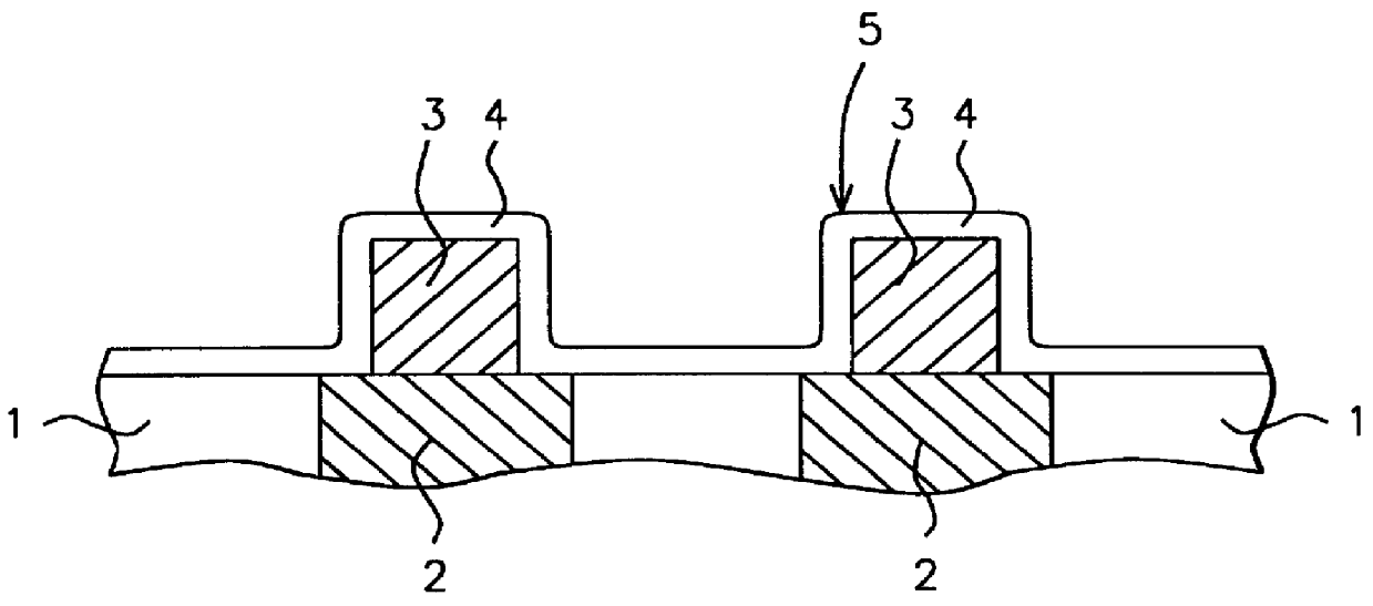
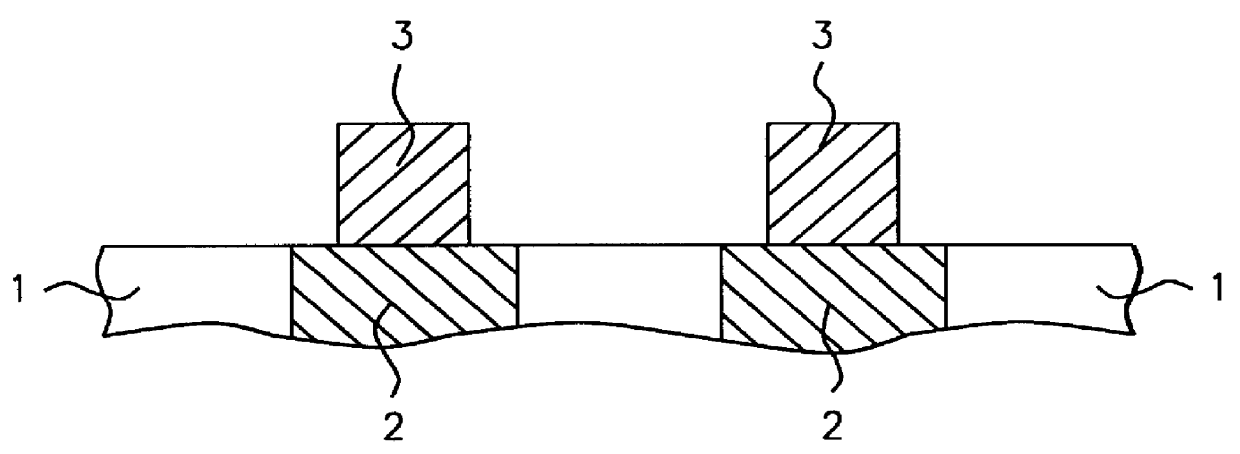
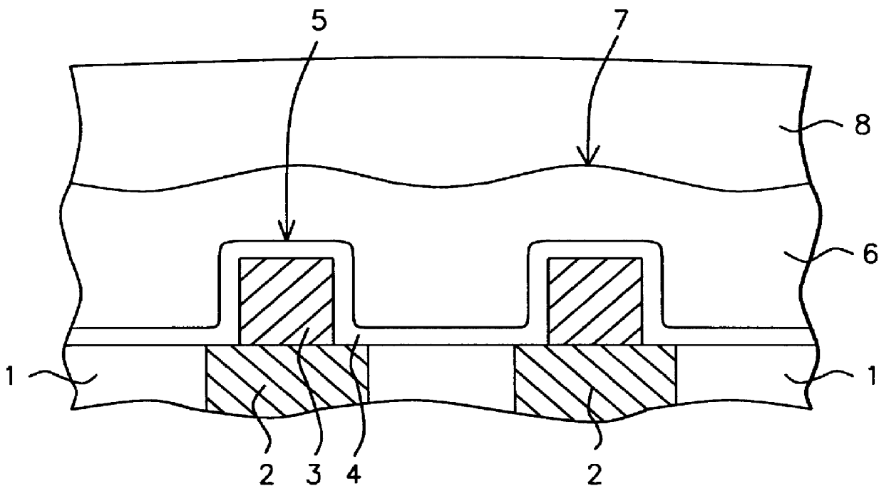
The method of forming a low k dielectric layer, with improved adhesion to an underlying insulator layer, featuring a series of nitrogen plasma treatments, performed prior to application of the low k dielectric layer, and prior to application, or deposition, of an insulator layer, overlying the low k dielectric layer, will now be described in detail. An underlying conductive region 2, comprised of either a metal interconnect structure, or a conductive, or active device region in a semiconductor substrate, encased in insulator layer 1, is schematically shown in FIG. 1 An overlying metal interconnect structure 3, comprised of a metal chosen from a group that includes aluminum, tungsten, or copper, is formed overlying, and contacting, underlying conductive regions 2. Metal interconnect structures 3, are formed via deposition of a metal layer, via either plasma vapor deposition, (PVD), or chemical vapor deposition, (CVD), procedures, at a thickness between about 150 to 1000 Angstroms. I...
PUM
Property
Measurement
Unit
thickness
aaaaa
aaaaa
pressure
aaaaa
aaaaa
temperature
aaaaa
aaaaa
Abstract
A process for forming an intermetal dielectric, (IMD), layer, comprised of an overlying silicon oxide layer, and an underlying low k dielectric layer, such as hydrogen silsesquioxane, (HSQ), has been developed. The process features the use of a series of plasma treatments, performed in a nitrogen containing ambient, used to improve the adhesion of the IMD layer, to underlying materials. A first plasma treatment is performed on a thin insulator layer, prior to application of the HSQ layer. The plasma treatment roughens the top surface of the thin insulator layer, resulting in improved adhesion of the HSQ layer to the thin insulator layer. A second plasma treatment is performed to the HSQ layer, prior to deposition of the overlying, thick silicon oxide layer, allowing improve adhesion of the thick silicon oxide layer, to the underlying HSQ layer, to be achieved.
Description
(1) Field of the InventionThe present invention relates to methods used to fabricate semiconductor devices, and more specifically to a method used to improve the adhesion of an intermetal dielectric, (IMD), layer, such as a hydrogen silsesquioxane, (HSG), layer, to underlying insulator layers.(2) Description of Prior ArtTo improve the performance of semiconductor chips, the RC, (resistance-capacitance), value, has to be decreased. The use of copper, for metal interconnect structures, has reduced the resistance component, of the RC value, when compared to more resistive metal interconnect structures, comprised with materials such as aluminum or tungsten. In addition, capacitance decreases have been achieved via use of low dielectric constant, (low k dielectrics), materials, such as hydrogen silsesquioxane, (HSQ), featuring a dielectric constant of about 2.9. HSQ layers are used to either replace silicon oxide layers, featuring a dielectric constant of about 3.9, or to be used as a co...
Claims
Application Information
Patent Timeline
Application Date:The date an application was filed.
Publication Date:The date a patent or application was officially published.
First Publication Date:The earliest publication date of a patent with the same application number.
Issue Date:Publication date of the patent grant document.
PCT Entry Date:The Entry date of PCT National Phase.
Estimated Expiry Date:The statutory expiry date of a patent right according to the Patent Law, and it is the longest term of protection that the patent right can achieve without the termination of the patent right due to other reasons(Term extension factor has been taken into account ).
Invalid Date:Actual expiry date is based on effective date or publication date of legal transaction data of invalid patent.