Active matrix type display device and fabrication method of the same

a liquid crystal display and active matrix technology, applied in static indicating devices, instruments, optics, etc., can solve problems such as the problem of operational balan

Inactive Publication Date: 2001-01-09
SEMICON ENERGY LAB CO LTD +1
View PDF19 Cites 35 Cited by
  • Summary
  • Abstract
  • Description
  • Claims
  • Application Information

AI Technical Summary

Benefits of technology

Another invention in which the above-mentioned structure is modified further is characterized, in that the region to which the impurity which gives N type conductivity is doped in the self-alignment process is composed of first regions formed adjacent to the source region and second regions formed adjacent to the drain region, the dimension of the first region is larger than a positioning accuracy in the non-self-alignment process during which the impurity which gives N type conductivity is doped, and the dimension of the second region is larger than that of the first region in the peripheral driving circuit portion. Thereby, high reliability may be given to the N-channel type driver portion without reducing its driving capability.

Problems solved by technology

It poses a problem in terms of the operational balance when a CMOS structure is adopted.
It poses a problem in the peripheral driving circuit in particular in which the CMOS structure is adopted.

Method used


Image

  • Active matrix type display device and fabrication method of the same
  • Active matrix type display device and fabrication method of the same
  • Active matrix type display device and fabrication method of the same

Examples


first embodiment

[First Embodiment]

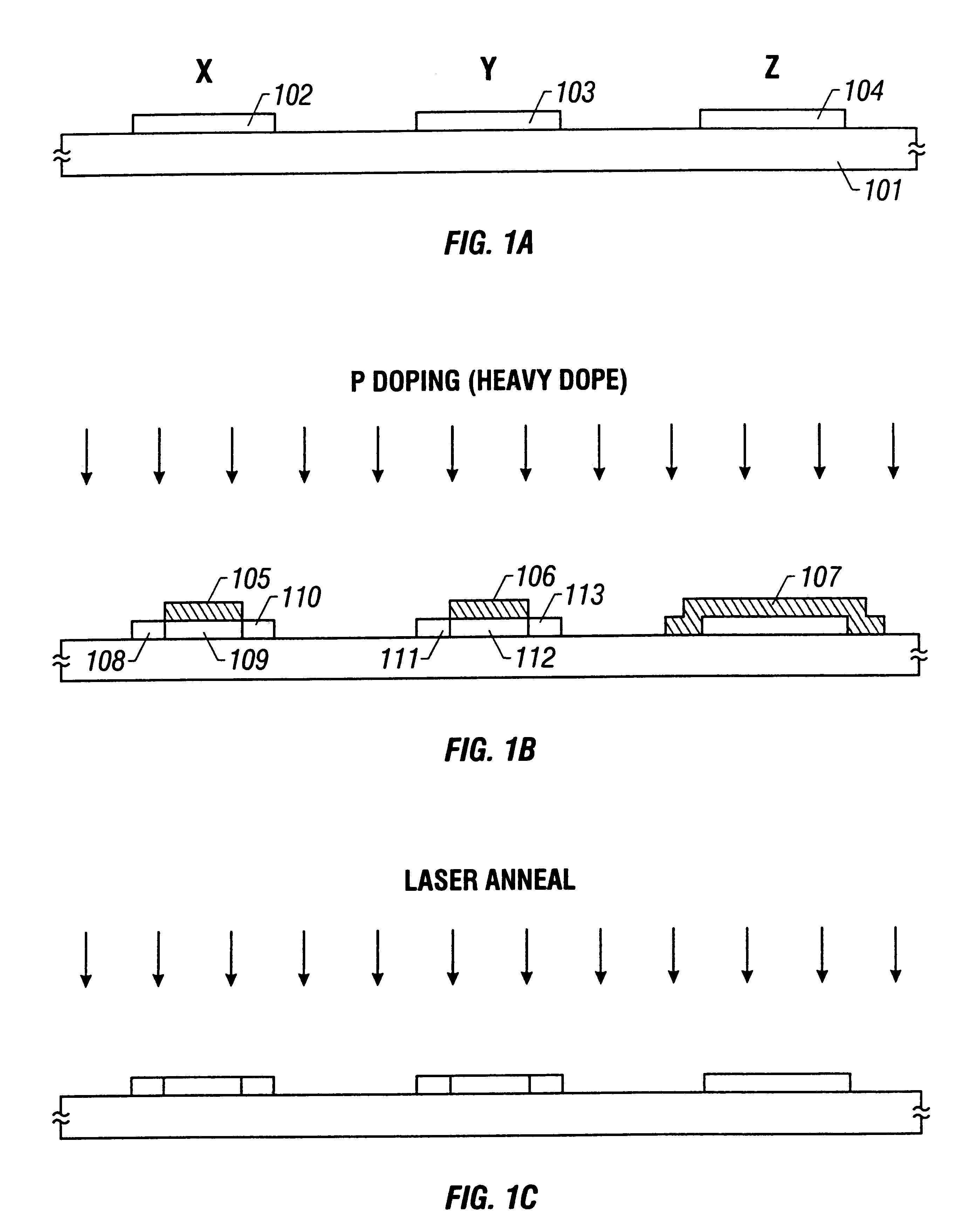
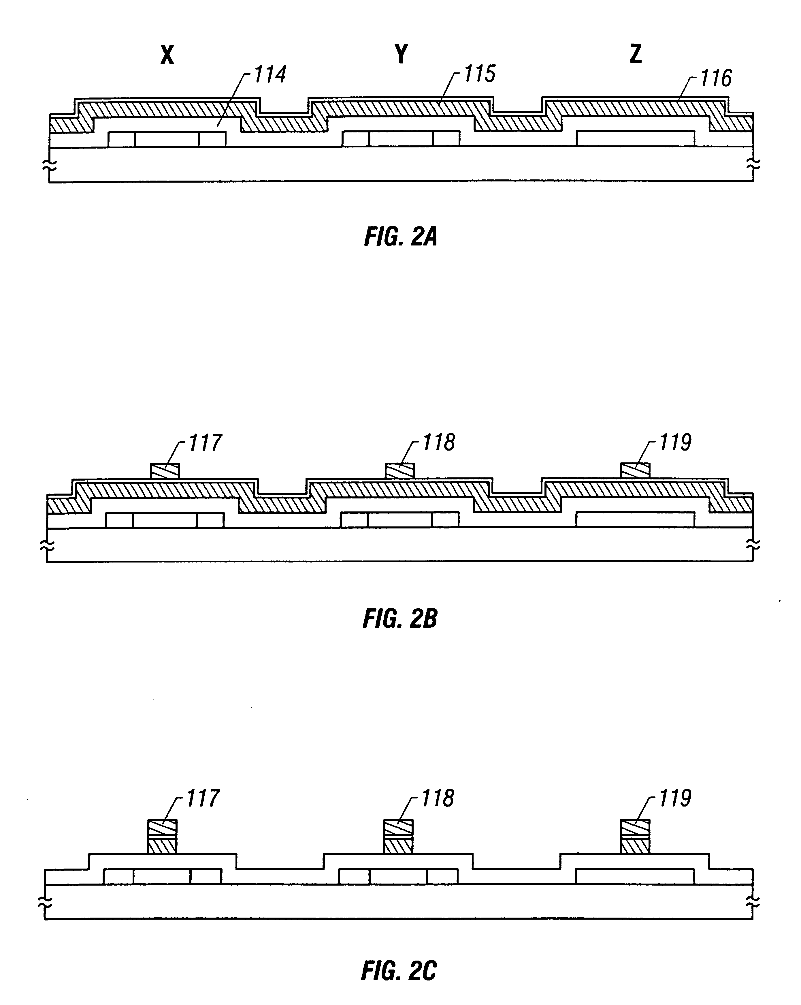
FIGS. 1 through 6 show steps for fabricating thin film transistors according to the first embodiment. Steps for fabricating the N-channel type thin film transistor provided in the pixel matrix portion X and the P- and N-channel type thin film transistors composing the driving circuit (buffer circuit) for driving the pixel matrix portion X on the same glass substrate will be described in the present embodiment.

In the figures, the N-channel type driver portion Y refers to the N-channel type thin film transistor portion composing the peripheral driving circuit. The P-channel type driver portion Z refers to the P-channel type thin film transistor portion composing the peripheral driving circuit.

A top gate type thin film transistor in which a gate electrode exists above an active layer is shown as a type of the thin film transistor in the present embodiment. However, the present invention can be also applied to a bottom gate type thin film transistor (an inverted stagge...

second embodiment

[Second Embodiment]

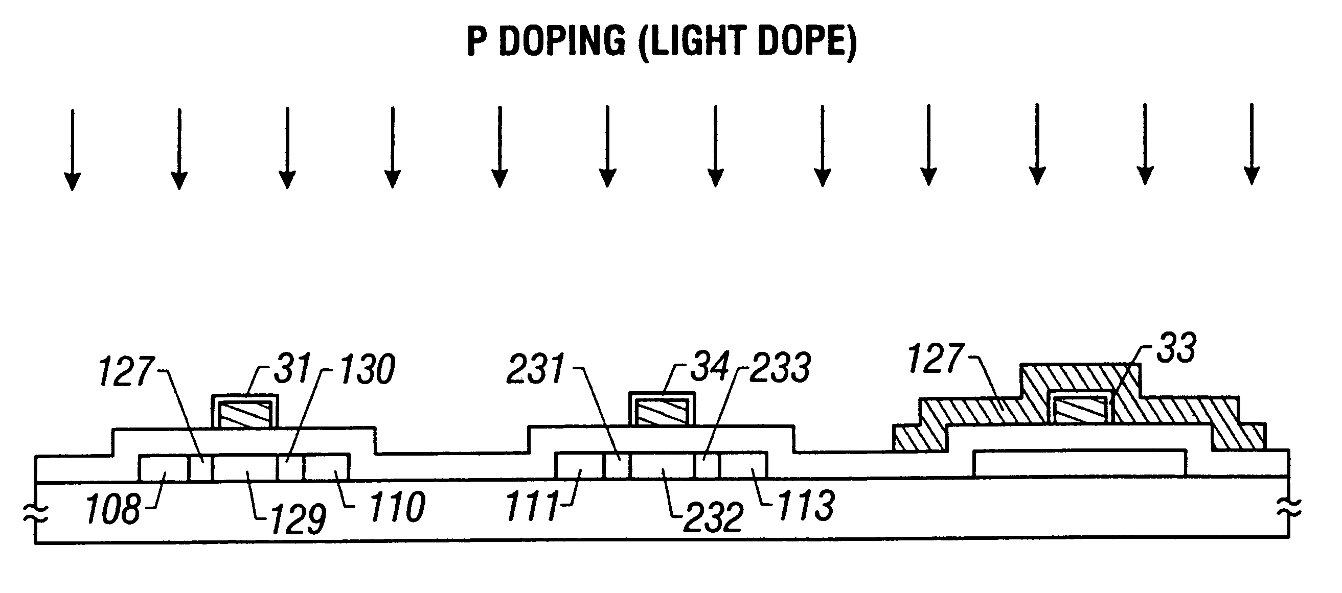
The present embodiment is what is the structure shown in the first embodiment is modified. The low concentrate impurity regions 131 and 133 having the same dimension have been provided in the N-channel type driver portion Y In the structure shown in the first embodiment (see FIG. 3B).

These low concentrate impurity regions have been provided in order to improve the reliability without dropping the high frequency characteristics and the driving capability as much as possible. However, the one which mainly exhibits its function (deterioration preventing function) is the low concentrate impurity region 133 adjacent to the drain region 113. Accordingly, the low concentrate impurity region 131 is not necessary in an extreme sense.

The low concentrate impurity region 131 may be considered to be existing just hampering the high frequency characteristics and the driving capability if no function of preventing the deterioration can be expected.

The present embodiment is chara...

third embodiment

[Third Embodiment]

The present embodiment relates to a structure in which one of the masks is reduced in the structure shown in the first embodiment.

FIGS. 10 and 11 show fabrication steps of the present embodiment. What is characterized in the present embodiment is that P is doped on the whole surface without using any resist mask in the step shown in FIG. 10B. This step corresponds to that shown in FIG. 3B.

In this step, P (phosphorus) which is the impurity which gives N-type is lightly doped to regions 11 and 13 which are to be source and region regions of the P-channel type thin film transistor. A region 12 is the region to which nothing is doped.

Then, B is doped only to the P-channel type driver portion Z in the step shown in FIG. 11A (heavy doping). In this step, the effect of P (phosphorus) lightly doped in the previous step is canceled by B heavily doped and the conductive type is inverted to P-type due to the effect of B excessively doped. Regions 234 and 236 are the P+ type r...


PUM

PropertyMeasurementUnit
thicknessaaaaaaaaaa
thicknessaaaaaaaaaa
thicknessaaaaaaaaaa

Abstract

There is provided an active matrix type display in which thin film transistors having required characteristics are provided selectively in a pixel matrix portion and a peripheral driving circuit portion. In a structure having the pixel matrix portion and the peripheral driving circuit portion on the same substrate, N-channel type thin film transistors having source and drain regions formed through a non-self-alignment process and low concentrate impurity regions formed through a self-alignment process are formed in the pixel matrix portion and in an N-channel driver portion of the peripheral driving circuit portion. A P-channel type thin film transistor in which no low concentrate impurity region is formed and source and drain regions are formed only through the self-alignment process is formed in a P-channel driver portion of the peripheral driving circuit portion.

Description

1. Field of the InventionThe present invention relates to a structure of an active matrix type liquid crystal display and more particularly to a structure of an active matrix type liquid crystal display into which a peripheral driving circuit is integrated.2. Description of Related ArtThere has been known an active matrix type liquid crystal display having a structure in which a thin film transistor is provided individually in each of several hundreds.times.several hundreds pixel electrodes provided in a matrix. The thin film transistor provided in each pixel has a function of controlling electric charge input / output to / from each pixel electrode.There has been also known one having a structure called a peripheral driving circuit integrated type in which a pixel matrix portion is integrated with a peripheral driving circuit on a same glass substrate. This peripheral driving circuit integrated structure is useful in that the production cost can be lowered and the whole structure can b...

Claims


Application Information

Patent Timeline
Patent Type & Authority Patents(United States)
IPC IPC(8): G02F1/136G02F1/1362G02F1/1368H01L21/336H01L21/77H01L21/84H01L29/786
CPCG02F1/13454H01L27/1214H01L27/1259H01L27/1288G02F1/136286G02F1/1368H01L27/124H01L29/66757
Inventor SHIBUYA TSUKASAYOSHINOUCHI ATSUSHIZHANG HONGYONGTAKENOUCHI AKIRA
Owner SEMICON ENERGY LAB CO LTD
Why Eureka
Try Eureka