Capacitively coupled field effect transistors for electrostatic discharge protection in flat panel displays

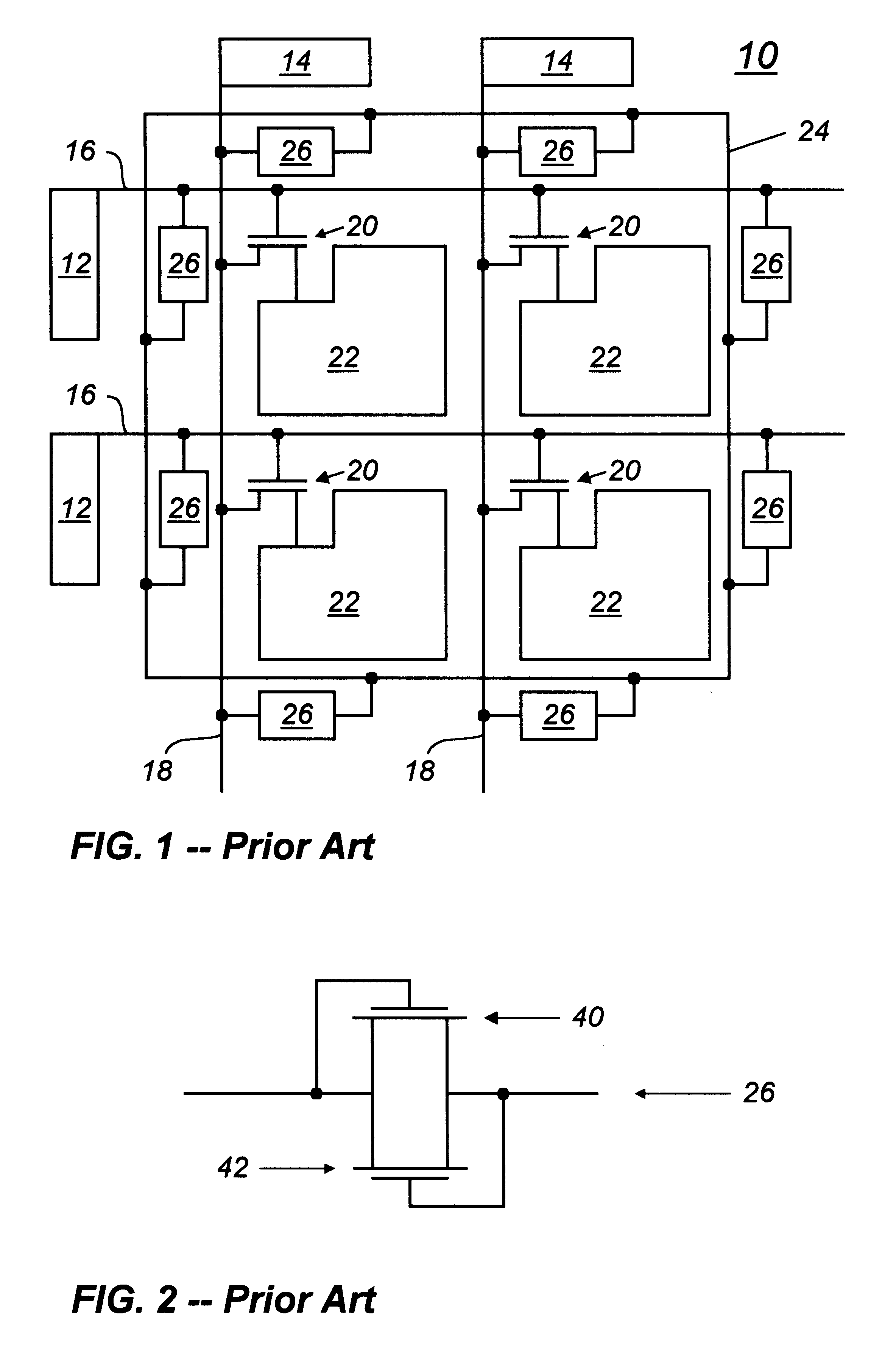
a field effect transistor and capacitive coupled technology, applied in the direction of semiconductor devices, semiconductor/solid-state device details, instruments, etc., can solve the problems of substantial drawbacks to the structure described the esd protection circuit illustrated in the holmberg patent provides inadequate protection from esd damage for the tn-lcd

Inactive Publication Date: 2001-01-16
AU OPTRONICS CORP
View PDF8 Cites 109 Cited by
  • Summary
  • Abstract
  • Description
  • Claims
  • Application Information

AI Technical Summary

Problems solved by technology

ESD might generate a large transient potential between a column line and a row line of a TN-LCD, in turn causing the breakdown of the silicon nitride of the TFT at the intersection between the column line and the row line.
There are substantial drawbacks to the structure described in the Holmberg patent.
As such, the ESD protection circuit illustrated in the Holmberg patent provides inadequate protection from ESD damage for the TN-LCD.
Two transistors must be provided to achieve an acceptable protection circuit element, but two transistors take up an undesirable amount of space.
Accordingly, the protection circuit element illustrated in Noguchi undesirably requires processing steps unnecessary to the formation of the rest of the display.
Accordingly, use of the ESD protection element illustrated in FIG. 2 increases the cost of flat panel displays and decreases yields slightly.

Method used


Image

  • Capacitively coupled field effect transistors for electrostatic discharge protection in flat panel displays
  • Capacitively coupled field effect transistors for electrostatic discharge protection in flat panel displays
  • Capacitively coupled field effect transistors for electrostatic discharge protection in flat panel displays

Examples


first embodiment

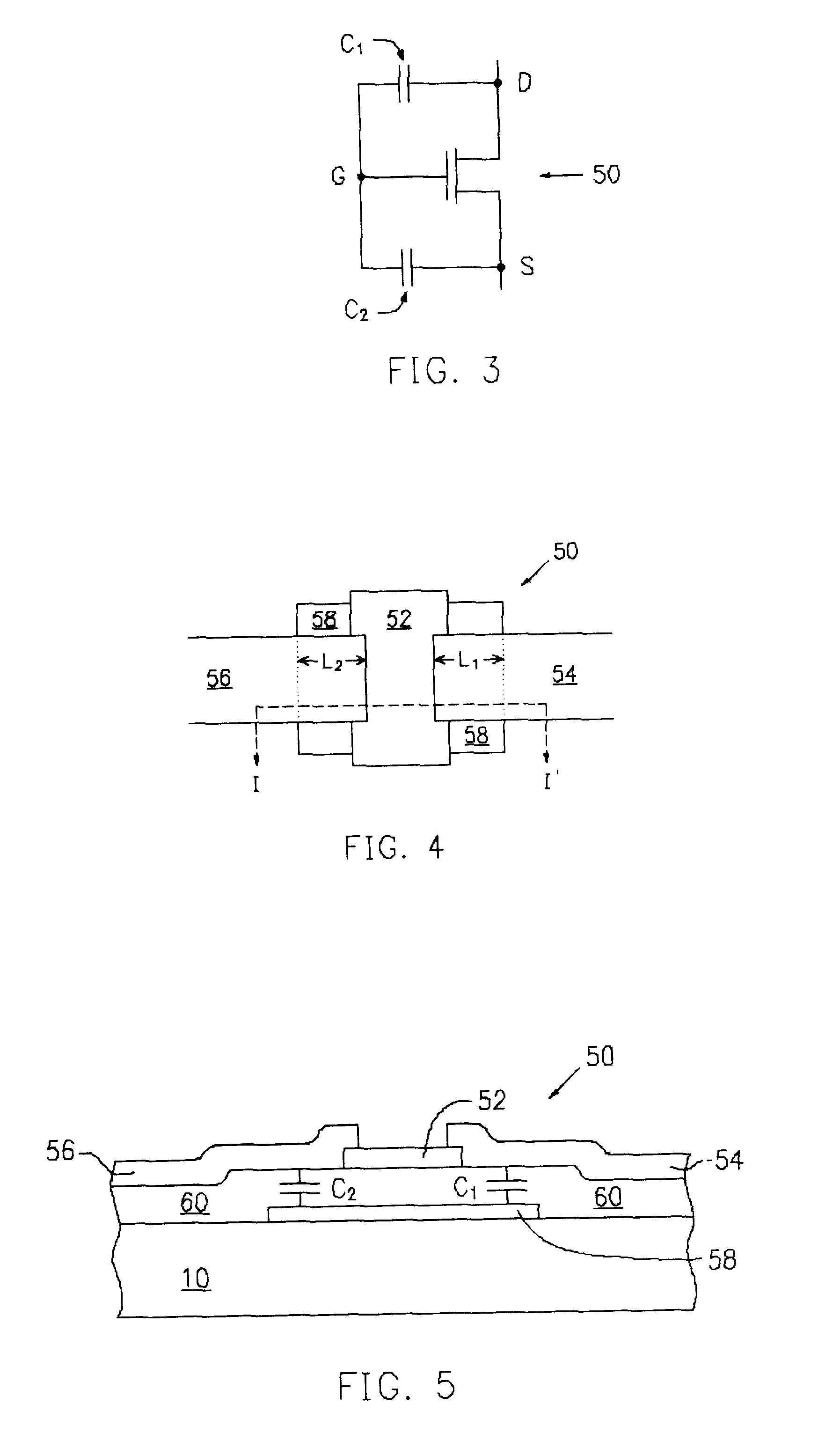
A different aspect of the first embodiment provides a second floating gate transistor in the protective circuit element, the second floating gate transistor having a floating gate, a drain and a source, with at least one of the drain and the source capacitively coupled to the floating gate. The drain of the first floating gate transistor is connected to the source of the second floating gate transistor and the source of the first floating gate transistor is connected to the drain of the second floating gate transistor.

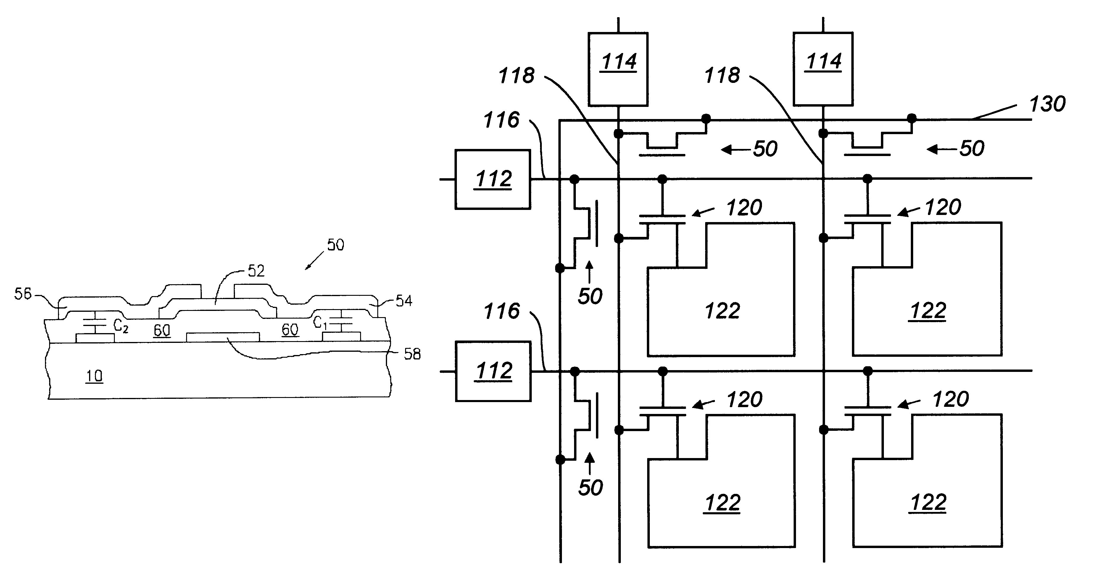
In accordance with a different aspect of the present invention, a flat panel display has a contact pad for providing a signal to a drive circuit, the drive circuit including at least one thin film transistor coupled to receive the signal provided at the contact pad, the thin film transistor generating a voltage to control a pixel of the flat panel display in response to the signal. A guard ring is provided adjacent to the contact pad. A capacitively coupled field effec...

second embodiment

A further aspect of this second embodiment provides that the gate of the capacitively coupled field effect transistor is connected to a first capacitor electrode and to a second capacitor electrode, the first capacitor electrode being disposed adjacent to a first wiring line connected to the drain so as to define a capacitive coupling between the gate and the drain, the second capacitor electrode being disposed adjacent to a second wiring line connected to the source so as to define a capacitive coupling between the gate and the source.

In accordance with another aspect of the invention, a flat panel display includes a plurality of parallel row select lines and a plurality of parallel column drive lines, the row select lines and the column drive lines intersecting to define a matrix of pixels. Pixel electrodes are provided at the intersections of the plurality of parallel column drive lines and the plurality of column select lines and a plurality of thin film transistors are each cou...


PUM

PropertyMeasurementUnit
dielectric constantaaaaaaaaaa
conductiveaaaaaaaaaa
capacitancesaaaaaaaaaa

Abstract

A flat panel display includes a plurality of parallel row select lines and a plurality of column drive lines, with the row select lines and the column drive lines intersecting to define a matrix of pixel locations. Signals are provided to contact pads located on the periphery of the display and the signals flow over the row select lines and the column drive lines to thin film transistors located adjacent a pixel electrode at each of the pixel locations. The signals provided to each thin film transistor cause the transistor to charge a corresponding pixel electrode to control a pixel of the display. ESD protection for the display comprises a guard ring adjacent the contact pads. Capacitively coupled field effect transistors (CCFETs) connect the row select lines to the guard ring and connect the column drive lines to the guard ring. A CCFET is formed as a thin film transistor and typically has a floating gate capacitively coupled to the drain and source of the thin film transistor.

Description

1. Field of the InventionThe present invention relates to the provision of electrostatic discharge (ESD) protection for flat panel displays incorporating thin film transistors (TFTs) in the pixel drive circuitry.2. Description of the Related ArtRecently, there has been growing commercial utilization of flat panel displays both as a replacement for the conventional CRT display and as a display for applications in which a CRT display is impractical, such as in portable computers and in viewers for video cameras. There are a variety of flat panel display technologies, including liquid crystal displays (LCDs), plasma displays and field emission displays. Of these, LCD technology has found the greatest level of acceptance in view of the comparative simplicity of the technology and the comparative ease of production. Flat panel displays are conventionally manufactured by forming electronic circuitry on an optically transparent substrate (e.g., glass) using photolithographic processing tec...

Claims


Application Information

Patent Timeline
Patent Type & Authority Patents(United States)
IPC IPC(8): G02F1/13G02F1/1362H01L29/66H01L27/12H01L29/786
CPCG02F1/136204H01L27/12H01L29/78696
Inventor WU, CHUNG-CHENGSAH, WEN-JYH
Owner AU OPTRONICS CORP
Why Eureka
Try Eureka