High frequency valid data strobe

a data strobe and high frequency technology, applied in the field of high speed memory, can solve the problems of insufficient phase locked loops and digital locked loops at such high speed operation, and the synchronization problems of high speed sram and dram memories between control signals and data signals

Inactive Publication Date: 2001-01-23
IBM CORP
View PDF9 Cites 58 Cited by
  • Summary
  • Abstract
  • Description
  • Claims
  • Application Information

AI Technical Summary

Problems solved by technology

Very high speed SRAM and DRAM memories have synchronization problems between control signals and data signals.
Phase locked loops and digital locked loops are not adequate at such high speed operation.

Method used


Image

  • High frequency valid data strobe
  • High frequency valid data strobe
  • High frequency valid data strobe

Examples


Embodiment Construction

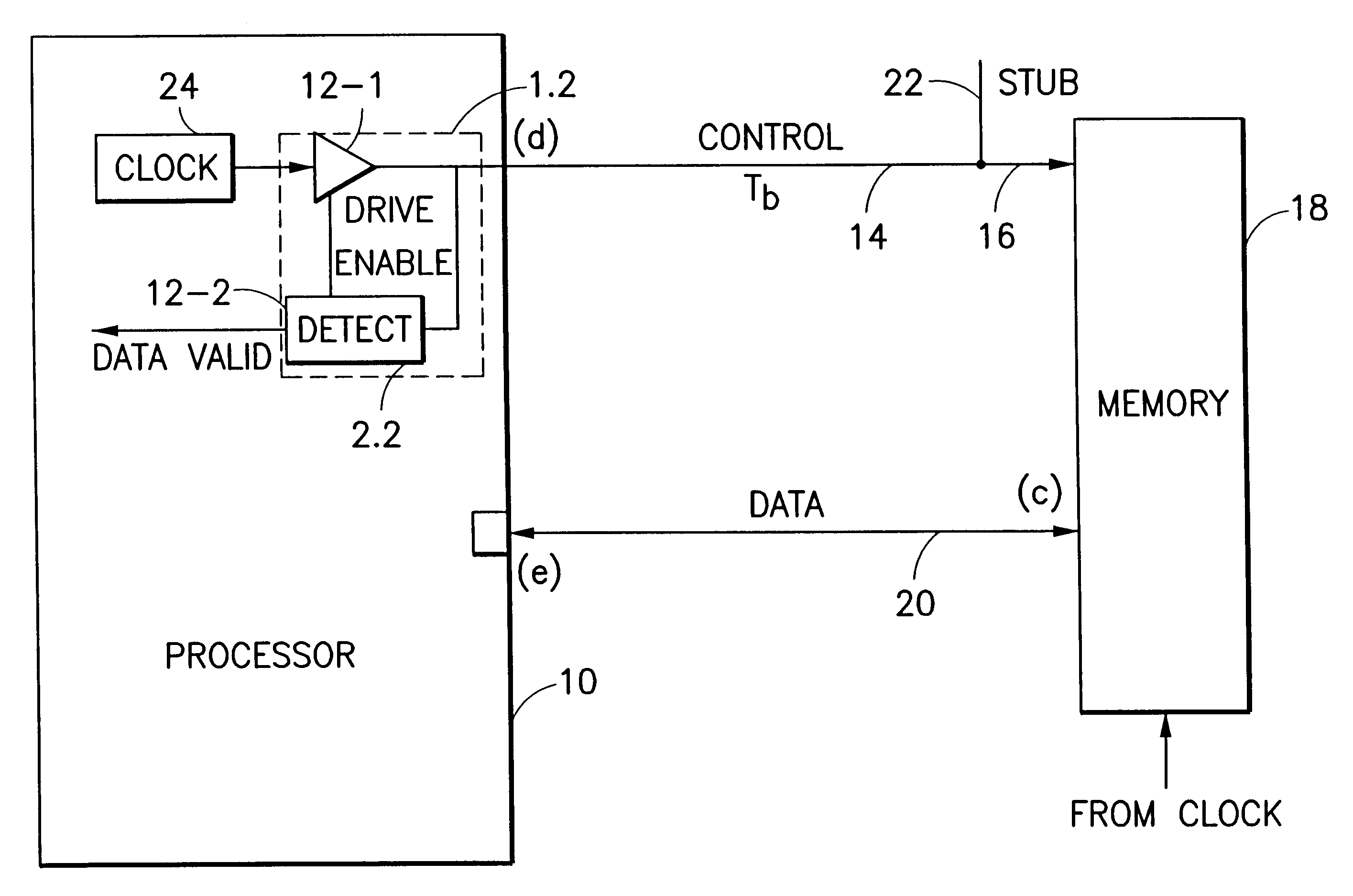
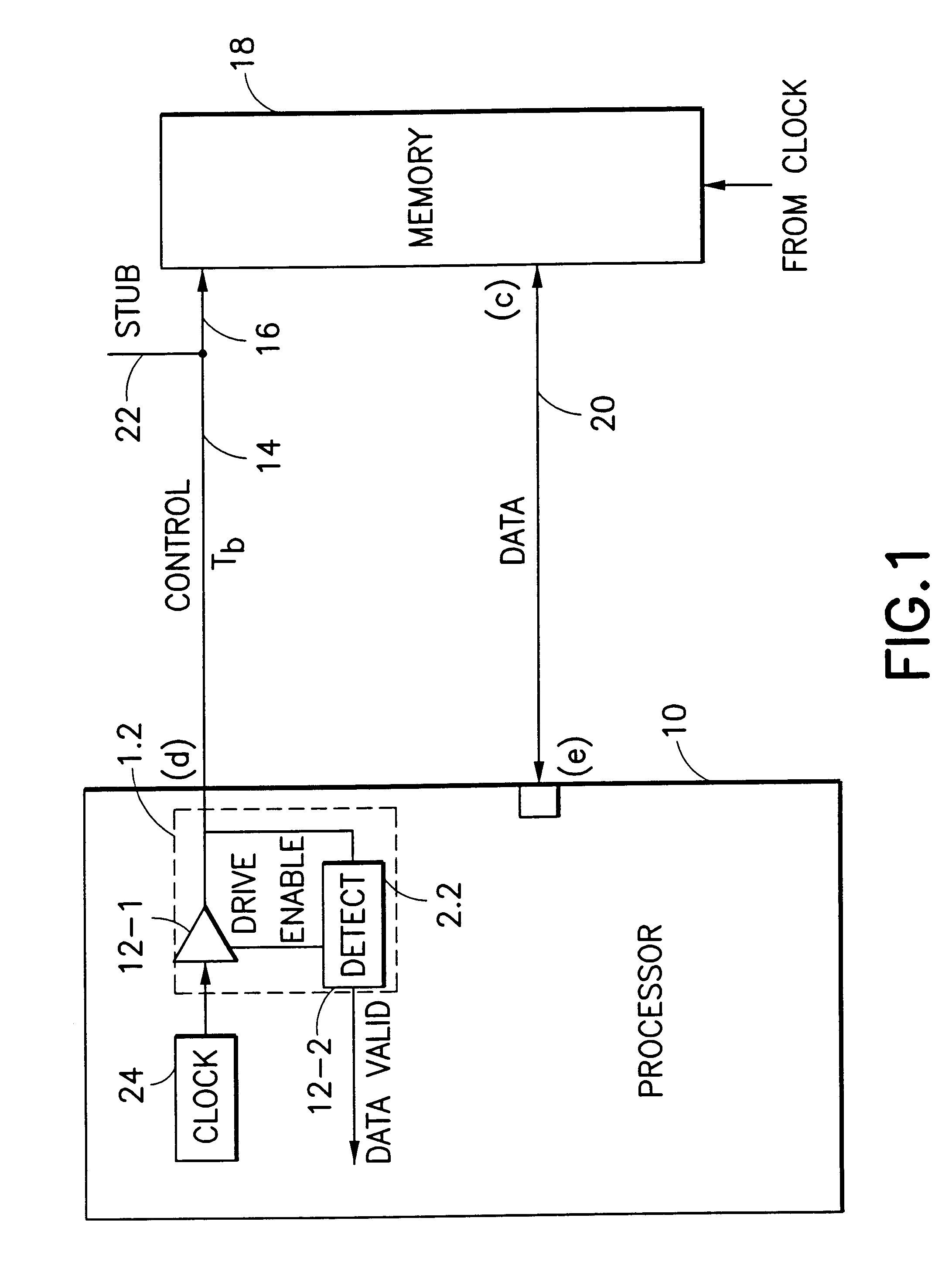
Very high speed operation of memories such as SRAMs and DRAMs results in synchronization problems occurring between control signals and data signals. Phase locked loops or digital locked loops do not perform adequately at such high speed operation.

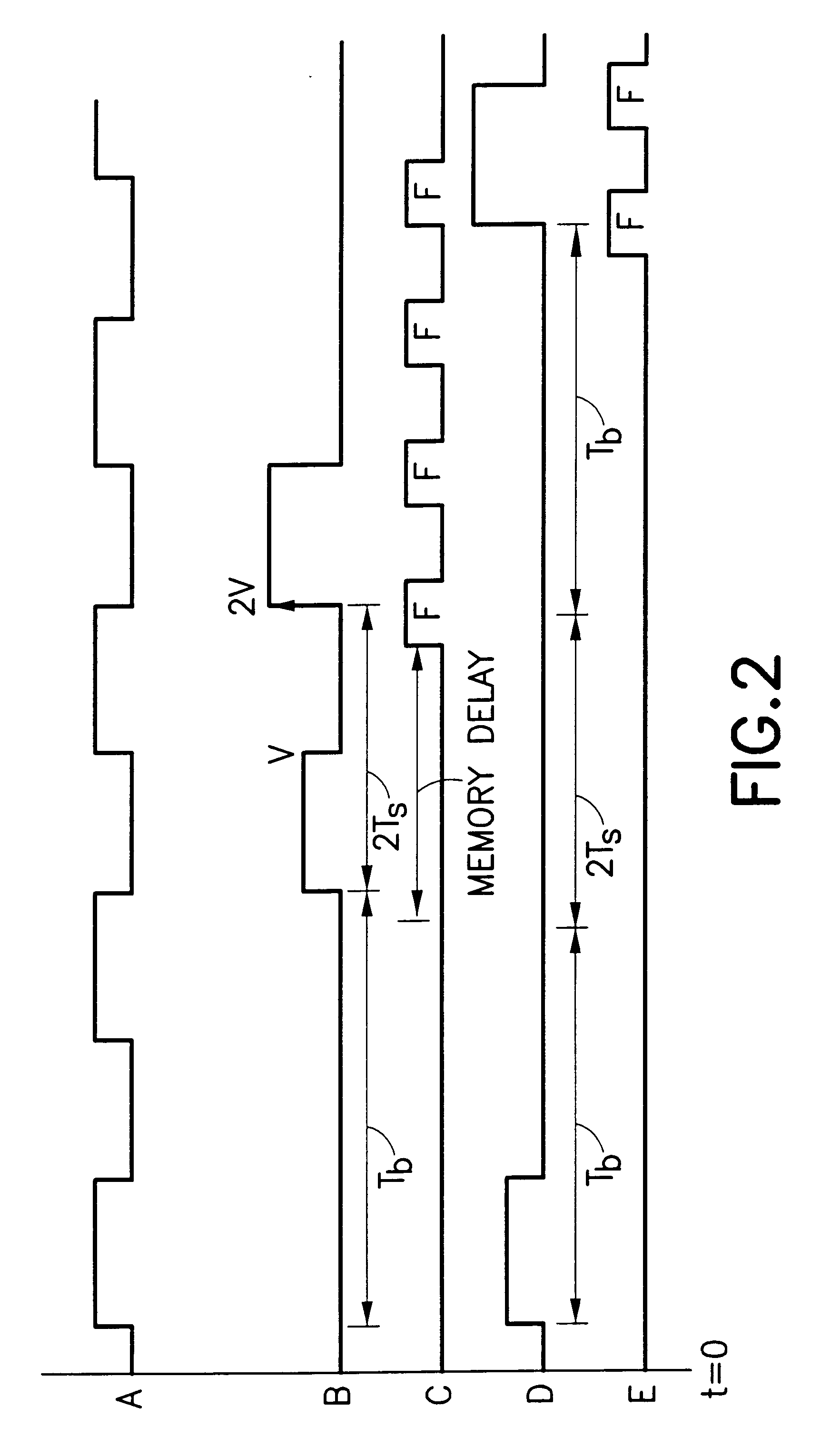
Transmission lines for memories have well controlled delays per unit lengths, and good high frequency characteristics. A delay line may be used to accurately set the time delay between control pulses and data pulses such that a data strobe occurs in synchronism with data arrival at the processor of the memory. For example, the strobe transition can be set to occur at the midpoint of the data valid window.

FIG. 1 shows a processor 10 with a memory send / received control circuit 12 including a bus drive circuit 12-1 connected to a processor clock 24 and a detector circuit 12-2 connected via control bus line 14 to the control input 16 of the memory 18. Detector circuit 12-2 is enabled by a signal from bus drive circuit 12-1. A data input line, ...


PUM


Abstract

A processor with a memory send/received control circuit including a bus drive circuit and a detector circuit connected via control bus line to the control input of the memory. A data input line, or output line, or data input/output line is connected between the processor and the memory. A transmission line stub having a length that is incrementally variable is connected to the memory control input side of the control line 14. The impedance Z0 of the transmission line stub is equal to that of the control line and is open circuited at the end which results in voltage doubling to achieve high speed synchronization between control signals and data signals and to ensure valid data at high clock rates.

Description

1. Field of the InventionThe present invention relates to high speed data transmission systems, and more particularly to a high speed memory including a stub at a variable end position.2. Background ArtVery high speed SRAM and DRAM memories have synchronization problems between control signals and data signals. Phase locked loops and digital locked loops are not adequate at such high speed operation.U.S. Pat. No. 5,457,406 issued Oct. 10, 1995 to Takada et al. entitled "Bidirectional Signal Transmission Circuit and Terminator" discloses a bidirectional signal transmission circuit in which the transmitter circuit of the logic circuit elements used in the conventional single end transmission circuit can be utilized by setting an impedance of an end circuit to be a value greater than a characteristic impedance of a transmission path, by shortening a length of the transmission path for connecting the end circuit with the logic circuit elements, and by increasing am amplitude of an input...

Claims


Application Information

Patent Timeline
Patent Type & Authority Patents(United States)
IPC IPC(8): G06F13/40H03K5/06H03K5/04
CPCG06F13/4086H03K5/06H04L25/0298
Inventor BERTIN, CLAUDE L.FIFIELD, JOHN A.HEDBERG, ERIK L.HOUGHTON, RUSSELL J.TONTI, WILLIAM R.
Owner IBM CORP
Why Eureka
Try Eureka