Electrical parameter evaluation system, electrical parameter evaluation method, and computer-readable recording medium for recording electrical parameter evaluation program

Inactive Publication Date: 2001-02-27
TOSHIBA MEMORY CORP
View PDF8 Cites 10 Cited by
  • Summary
  • Abstract
  • Description
  • Claims
  • Application Information

AI Technical Summary

Problems solved by technology

However, in the silicon MOSFET, a two-dimensional quantization effect of conductive carriers as a quantum-mechanical effect cannot be disregarded because of the thinner thickness of the gate oxide film and the higher concentration in the silicon substrate according to miniaturization of the device.
In other words, a high precision simulation has been going to become difficult in the device simulator using the classical theory.
Since such difference in the inversion layer capacitance cannot be disregarded, high precision simulation carried out by the device simulator based on the classical theory has been going to become difficult.
This method can provide the most strict solution, but it has defects such that an extremely long time is required for calculation rather than the classical theory and that two-dimensional analysis and three-dimensional analysis which are indispensable for evaluation of a short channel effect, etc. are difficult.
Such methods are infer

Method used


Image

  • Electrical parameter evaluation system, electrical parameter evaluation method, and computer-readable recording medium for recording electrical parameter evaluation program
  • Electrical parameter evaluation system, electrical parameter evaluation method, and computer-readable recording medium for recording electrical parameter evaluation program
  • Electrical parameter evaluation system, electrical parameter evaluation method, and computer-readable recording medium for recording electrical parameter evaluation program

Examples


first embodiment

(First Embodiment)

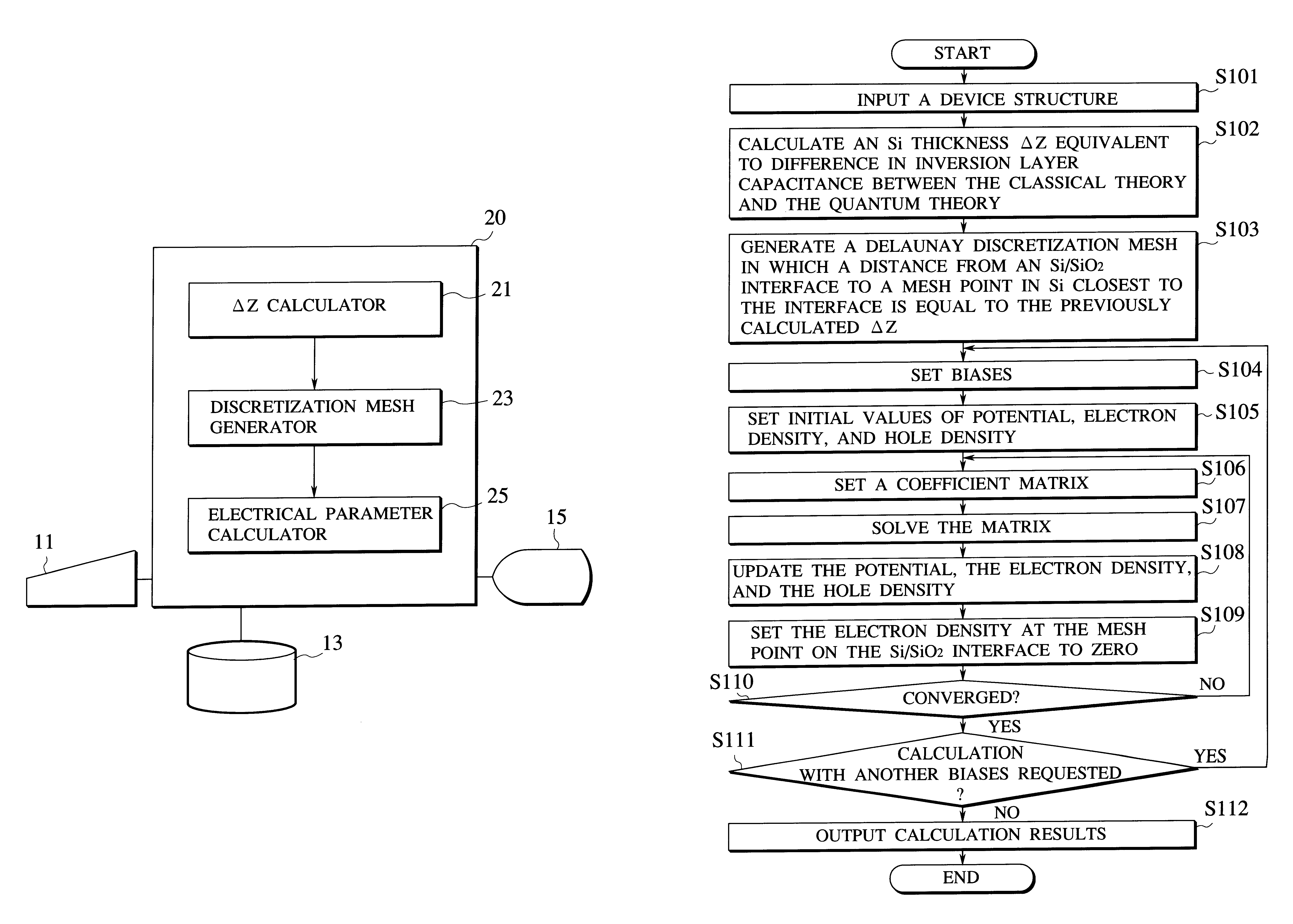
FIG. 5 is a block diagram showing an electrical parameter evaluation system according to the present invention. The electrical parameter evaluation system can input device structure information of a semiconductor device and channel conductivity type information on an interface between a gate insulating film and a semiconductor substrate from an inputting means 11 as input data, store the input data into a memory means 13, calculate difference between an inversion layer capacitance by the classical theory and an inversion layer capacitance by the quantum theory and calculate .DELTA.Z which is a thickness of the semiconductor substrate equivalent to the difference in inversion layer capacitance by a .DELTA.Z calculator 21, and store the .DELTA.Z into the memory means 13. Then, the electrical parameter evaluation system can generate the Delaunay discretization mesh for the structure of the semiconductor device to be evaluated by a discretization mesh generator 23, and...

second embodiment

(Second Embodiment)

Next, an electrical parameter evaluation method according to a second embodiment of the present invention will be explained with reference to FIGS. 10 and 11. As has been shown in the first embodiment, one-dimensional MISFET device simulation may be carried out by solving the Poisson equation. However, in order to execute two-dimensional or three-dimensional electrical parameter evaluation, not only the Poisson equation but also an electron or hole continuous equation (current flow equation) must be solved. As an example to implement the above, a flowchart for two-dimensional analysis of the N-type MOSFET is shown in FIG. 10. The flowchart illustrative of the second embodiment differs from the flowchart illustrative of the first embodiment only in the process in step S206. Accordingly, the process in step S206 which generates the coefficient matrix under an assumption that electron current of the mesh points on the Si / SiO.sub.2 interface is set to zero will be exp...

third embodiment

(Third Embodiment)

Next, an electrical parameter evaluation method according to a third embodiment of the present invention will be explained with reference to FIG. 12. In the third embodiment, the case where electrical parameters of a device shown in FIG. 12 are calculated numerically will be thought of. The device shown in FIG. 12 has the interface between the insulator and the semiconductor substrate 108 from an interface 101 to an interface 105. Out of these interfaces, the interface between the gate oxide film and the semiconductor substrate 108 is the interface 103. Therefore, two-dimensional quantization of the carrier occurs at the interface 103, nevertheless two-dimensional quantization does not occur at remaining interfaces. As a result, a two-dimensional quantization effect must be considered only at the interface 103 between the insulator and the semiconductor substrate 108.

If the present invention is applied partially, for example, procedures will be taken as follows. As...


PUM


Abstract

A DELTAZ calculator calculates difference between an inversion layer capacitance by a classical theory and an inversion layer capacitance by a quantum theory, calculates DELTAZ which is a thickness of a semiconductor substrate equivalent to the difference in inversion layer capacitance. A discretization mesh generator generates a Delaunay discretization mesh for a structure of the semiconductor device to be evaluated. An electrical parameter calculator calculates electrical parameters of the semiconductor device under constraint that a charge density of channel conductivity type of the semiconductor device is set to zero at discretization mesh points of the discretization mesh on an interface between an insulating film and the semiconductor substrate and at discretization mesh points of the discretization mesh in the semiconductor substrate which are located within a distance less than the stored DELTAZ from the interface between the insulating film and the semiconductor substrate.

Description

1. Field of the InventionThe present invention relates to an electrical parameter evaluation system, an electrical parameter evaluation method, and a computer-readable recording medium for recording an electrical parameter evaluation program and, more particularly, a technique for evaluating electrical parameters of MISFET with the use of the Delaunay discretization scheme, which is capable of taking the quantum-mechanical effect in account approximately by a calculation time equivalent to that required for the simulator with the use of the classical theory and also is applicable to a case impurity distribution in a semiconductor substrate is not uniform.2. Description of the Related ArtIn the prior art, in a device simulator which executes electrical parameter evaluation of MISFET represented by a silicon MOSFET numerically by virtue of numerical calculation, Boltzmann statistics based on the classical theory has been employed as the carrier distribution. However, in the silicon MO...

Claims


Application Information

Patent Timeline
IPC IPC(8): G06F17/50H01L29/00H01L21/336H01L29/78
CPCG06F17/5018G06F2217/16G06F30/23G06F2111/10
Inventor TANIMOTO, HIROYOSHIENDA, TOSHIYUKISHIGYO, NAOYUKIMATSUZAWA, KAZUYA
Owner TOSHIBA MEMORY CORP
Why Eureka
Try Eureka