Device and process for reading a matrix of photonic detectors

a technology of photonic detectors and matrixes, which is applied in the direction of radio frequency controlled devices, instruments, television systems, etc., can solve the problems of preventing the production of sub-images, reading circuits, and incompatibility with random addressing of detectors

Inactive Publication Date: 2001-03-13
COMMISSARIAT A LENERGIE ATOMIQUE ET AUX ENERGIES ALTERNATIVES
View PDF3 Cites 20 Cited by
  • Summary
  • Abstract
  • Description
  • Claims
  • Application Information

AI Technical Summary

Benefits of technology

The invention makes it possible to simplify the electronics of a read circuit by eliminating the reset devices present in the elementary points even in the devices of the prior art. This function is nevertheless kept but is performed by a charge amplifier external to the elementary point except in one of the particular cases of the linear array of detectors where the amplifier is situated within the elementary point.
finally, the invention makes it possible to implement read circuits with a CMOS technology which has the particularity of affording both high integration density and random reading of the detectors, unlike the devices of the prior art implemented with a CCD technology.

Problems solved by technology

On the other hand, they are not compatible with a random addressing of the detectors, which prevents the production of sub-images.
Finally, these read circuits have the major drawback of having to be implemented in specific networks whose integration density is lower than that of conventional CMOS networks whereas the pitch of the detector mosaics is greatly reduced.
A first limitation is related to the detector read mode.
This function therefore imposes additional constraints in the design of the elementary point, and the smaller the pitch of the elementary point, the more difficult it will be to meet these.
The reduction in the storable charge then results in a degradation of the signal to noise ratio.
Another limitation of this type of architecture is related to the reading rate, which imposes sizing constraints on the voltage amplifier of the elementary point and on the switch which affords a connection between the outputs of elementary points in one and the same column to the output amplifier.
These constraints become all the more difficult to satisfy as the number of detectors increases and the pitch of the elementary points decreases whilst the image rate remains constant and the number of outputs rather has a tendency to decrease.
This point may be prohibitive in terms of signal to noise ratio for circuits of large size, and therefore with a high Cbc, and / or for applications where the charge to be manipulated is small.
On the other hand, it is clear that this type of architecture is not compatible with an identical and synchronous exposure time for all the elementary points.
The problem is to design an elementary point which makes it possible to read the signal delivered by a mosaic of quantal detectors or thermal detectors, knowing that the following are necessary:

Method used


Image

  • Device and process for reading a matrix of photonic detectors
  • Device and process for reading a matrix of photonic detectors
  • Device and process for reading a matrix of photonic detectors

Examples


Embodiment Construction

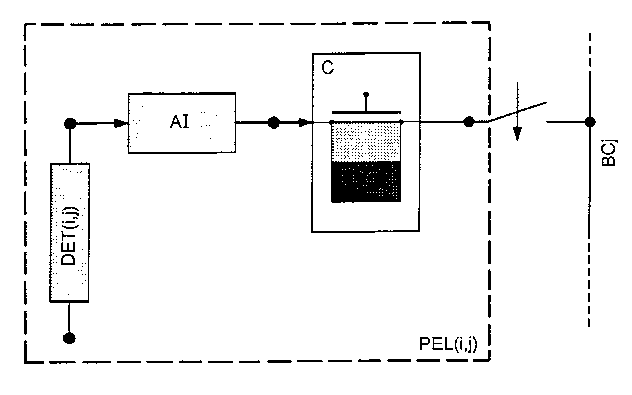
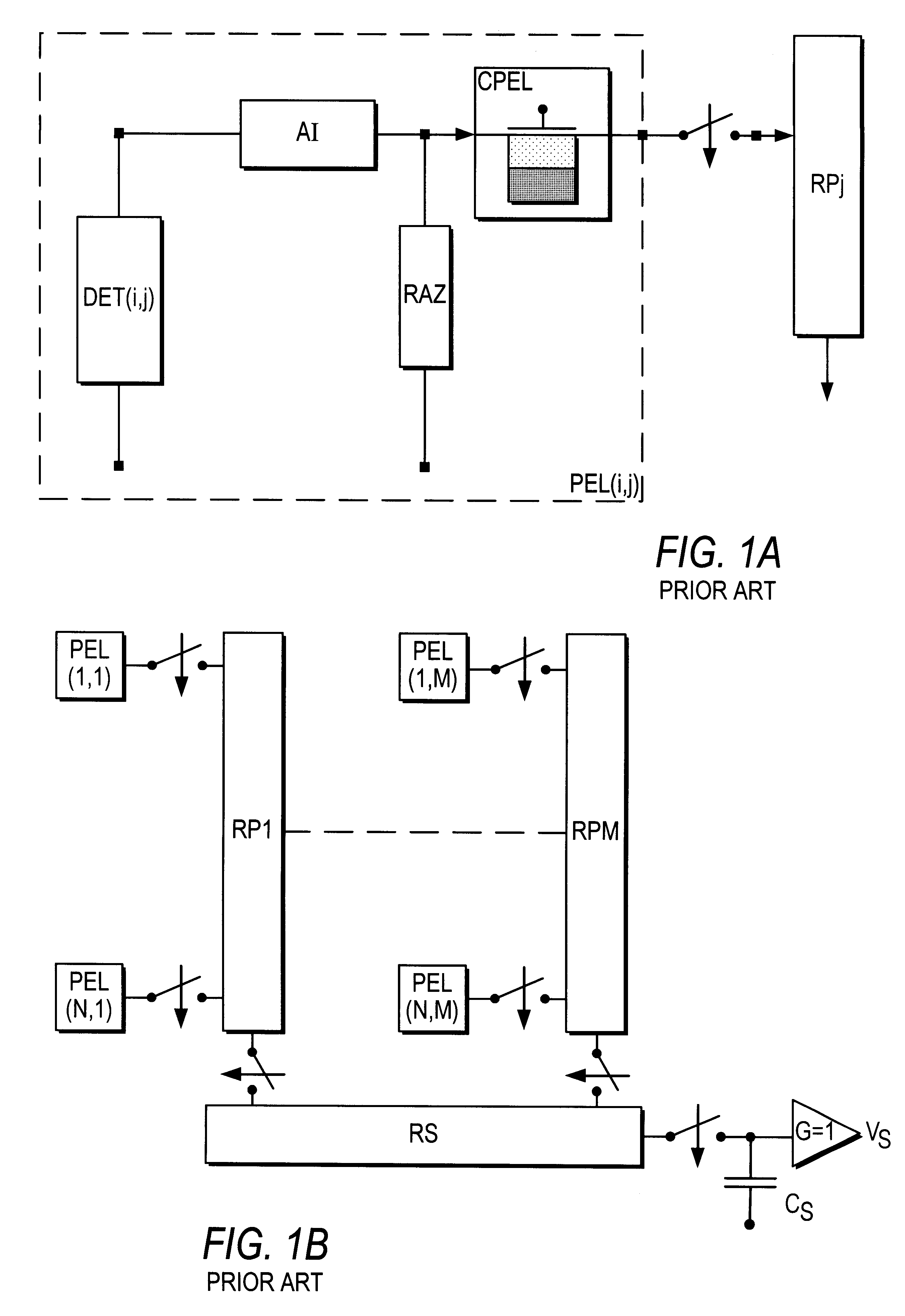
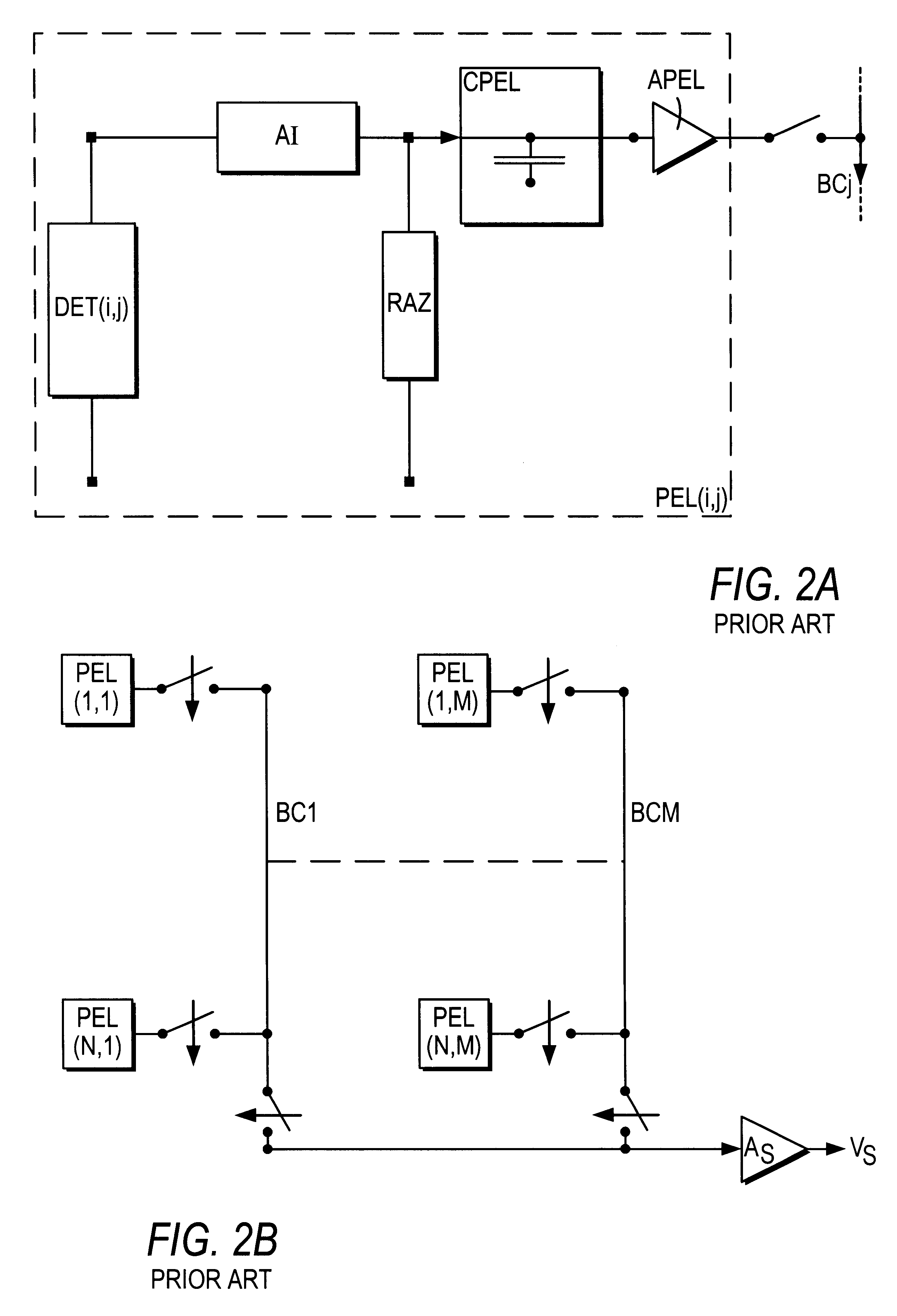
The present invention concerns a device for reading a matrix of photonic detectors which delivers a current whose intensity varies according to the incident flux, the exposure time being identical and synchronous for all the detectors, characterised in that it comprises a set of elementary points for reading the signals delivered by each detector, in that the quantity processed is the charge, each elementary point effecting a preintegration of the current delivered by a corresponding detector. A reading of the resulting quantity of charges by a charge amplifier is effected, so as to condition the signals delivered by the matrix of detectors and to multiplex them to at least one information processing chain. The charge amplifier is external to the elementary point in the case of a matrix of detectors. In the case of a linear array of detectors, the charge amplifier is situated either outside or inside the elementary point.

Advantageously, the photonic detectors are quantal detectors o...


PUM


Abstract

A method and a device are provided for reading a matrix of photonic detectors which delivers a current whose intensity varies according to the incident flux. A set of elementary points (PEL(i,j)) enables the signals delivered by each detector to be read. The quantity processed is the charge. Each elementary point effects a preintegration of the current delivered by a corresponding detector. A charge amplifier effects a reading to condition the signals delivered by the matrix of detectors and to multiplex them to at least one information processing chain.

Description

DESCRIPTION1. Technical FieldThe present invention relates to a device for reading a matrix of photonic detectors.2. Prior ArtThe photonic detection devices to which the invention relates are of two types:quantal;thermal.In quantal detectors, the photons received by the detector are converted into electrons and / or holes according to the detection principle, which may be intrinsic (direct transition from valence band to conduction band) or extrinsic (transition between intermediate level and conduction band). Quantal detectors can be grouped into two categories:photovoltaic detectors, whose current intensity varies according to the incident flux;photoconductive detectors, whose resistance varies according to the incident flux.Thermal detectors can be grouped into two categories:resistive bolometric detectors, whose resistance varies according to the energy of the incident radiation;diode detectors, whose current intensity varies according to the incident flux.Quantal detectors and th...

Claims


Application Information

Patent Timeline
Patent Type & Authority Patents(United States)
IPC IPC(8): H01L27/146H04N3/15H04N5/33H04N5/335H04N5/3745
CPCH01L27/14603H04N3/1512H04N5/3745H04N25/77H04N25/771H04N25/76
Inventor MARION, DOMINIQUEMOTTIN, ERICPANTIGNY, PHILIPPE
Owner COMMISSARIAT A LENERGIE ATOMIQUE ET AUX ENERGIES ALTERNATIVES
Why Eureka
Try Eureka