Check patentability & draft patents in minutes with Patsnap Eureka AI!

Single event upset (SEU) hardened static random access memory cell

a memory cell and single event technology, applied in static storage, information storage, digital storage, etc., can solve the problems of high processing cost of soi, single event upset (seus) or soft errors, and the logic state of the sram cell will be ups

Inactive Publication Date: 2001-03-27
BAE SYST INFORMATION & ELECTRONICS SYST INTERGRATION INC
View PDF19 Cites 29 Cited by
  • Summary
  • Abstract
  • Description
  • Claims
  • Application Information

AI Technical Summary

Problems solved by technology

In certain environments, such as satellite orbital space, in which the level of radiation is relatively intense, electronic devices that utilize static random access memories (SRAMs) are more susceptible to single event upsets (SEUs) or soft errors.
Should the energetic particle generate a critical charge within a storage node of an SRAM cell, the logic state of the SRAM cell will be upset.
However, the processing cost of SOI is much higher than bulk silicon; thus, SOI is generally not the most preferable method.
But as the number and density of memory cells and logic circuits within an integrated circuit device have rapidly grown over the years, SEU error rate has become an alarming problem that cannot be ignored, even for application environments in which the level of radiation is relatively low.
But this increase in RC propagation delay also slows the write cycle time of SRAM cell 20.
However, as memory cells are scaled to smaller geometries, the speed of the write cycle of SRAM cells becomes more critical than in previous SRAM designs.
In addition, it is very difficult to control process parameters under the resistive approach.
As a result, the resistive approach to SEU hardening is no longer desirable for SRAMs.
Furthermore, the increased capacitance on the gate will increase the RC delay in the feedback path, thus increasing the resistance to SEUs as well as retarding changes in logic state.
However, the capacitive approach to SEU hardening is not very practical because it slows down the speed of the memory cell.

Method used


Image

  • Single event upset (SEU) hardened static random access memory cell
  • Single event upset (SEU) hardened static random access memory cell
  • Single event upset (SEU) hardened static random access memory cell

Examples


Embodiment Construction

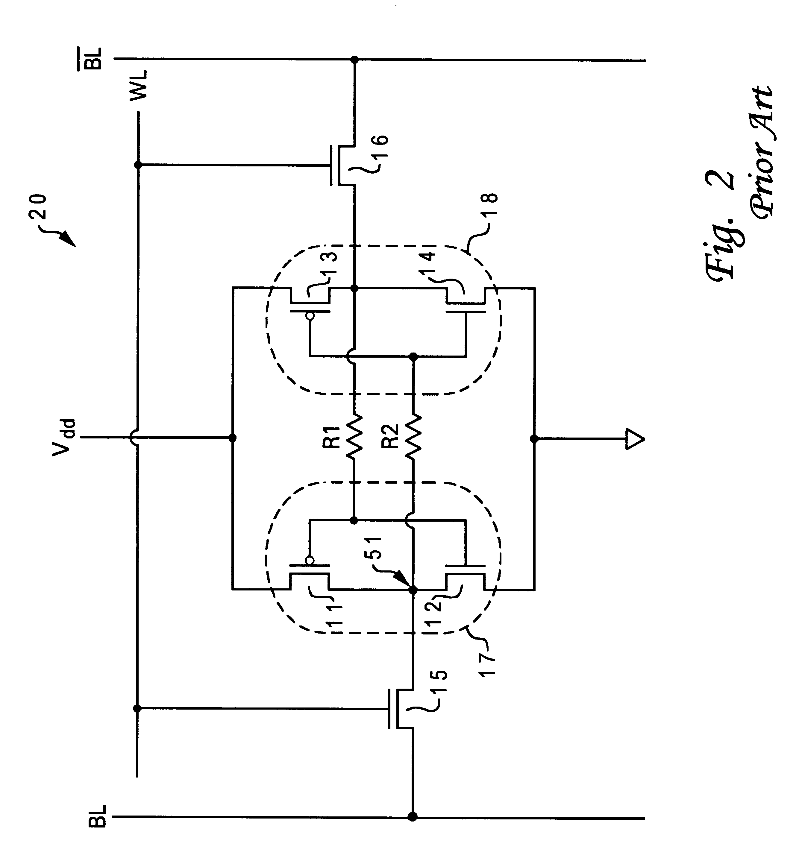
With reference now to FIG. 4, there is illustrated a schematic diagram of an SEU-hardened SRAM cell in accordance with a preferred embodiment of the present invention. As shown, an SRAM cell 40 includes p-channel transistors 41-44 and n-channel transistors 47-50. Transistors 41, 42, 47, and 48 are connected in series, with the source of transistor 41 connected to a power supply, V.sub.dd, and transistor 48 connected to ground. Similarly, transistors 43, 44, 49, and 50 are connected in series, with the source of transistor 43 connected to V.sub.dd and transistor 50 connected to ground.

In addition, transistors 41, 42 are cross-coupled to transistors 43, 44, and transistors 47, 48 are cross-coupled to transistors 49, 50. For transistors 41-44, the cross-coupling is accomplished by connecting the gate of transistor 41 to a node between transistors 43 and 44, and by connecting the gate of transistor 43 to a node between transistors 41 and 42. For transistors 47-50, the cross-coupling is ...


PUM


Abstract

A single event upset hardened memory cell to be utilized in static random access memories is disclosed. The single event upset hardened memory cell includes a first set of cross-coupled transistors, a second set of cross-coupled transistors, a first set of isolation transistors, and a second set of isolation transistors. The first and second sets of isolation transistors are coupled to the first and second set of cross-coupled transistors, respectively, such that two inversion paths are formed between the cross-coupled transistors and the isolation transistors.

Description

1. Technical FieldThe present invention relates to integrated circuits in general, and in particular to bi-stable integrated circuits. Still more particularly, the present invention relates to a single event upset hardened memory cell to be utilized in static random access memories.2. Description of the Prior ArtIn certain environments, such as satellite orbital space, in which the level of radiation is relatively intense, electronic devices that utilize static random access memories (SRAMs) are more susceptible to single event upsets (SEUs) or soft errors. These SEUs are typically caused by electron-hole pairs created by, and travelling along the path of, a single energetic particle as it passes through the memory cells of the SRAMs. Should the energetic particle generate a critical charge within a storage node of an SRAM cell, the logic state of the SRAM cell will be upset. Thus, the critical charge is the minimum amount of electrical charge required to change the logic state of t...

Claims


Application Information

Patent Timeline
IPC IPC(8): G11C11/412
CPCG11C11/4125
Inventor PHAN, HO GIAJALLICE, DERWINLI, BINHOFFMAN, JOSEPH
Owner BAE SYST INFORMATION & ELECTRONICS SYST INTERGRATION INC
Features
  • R&D
  • Intellectual Property
  • Life Sciences
  • Materials
  • Tech Scout
  • Unparalleled Data Quality
  • Higher Quality Content
  • 60% Fewer Hallucinations
Learn More