Command-controllable IC memory with compatibility checking unit suspending memory operation/enabling data to be only read from memory when IC memory operation is host incompatible
- Summary
- Abstract
- Description
- Claims
- Application Information
AI Technical Summary
Benefits of technology
Problems solved by technology
Method used
Image
Examples
embodiment 1
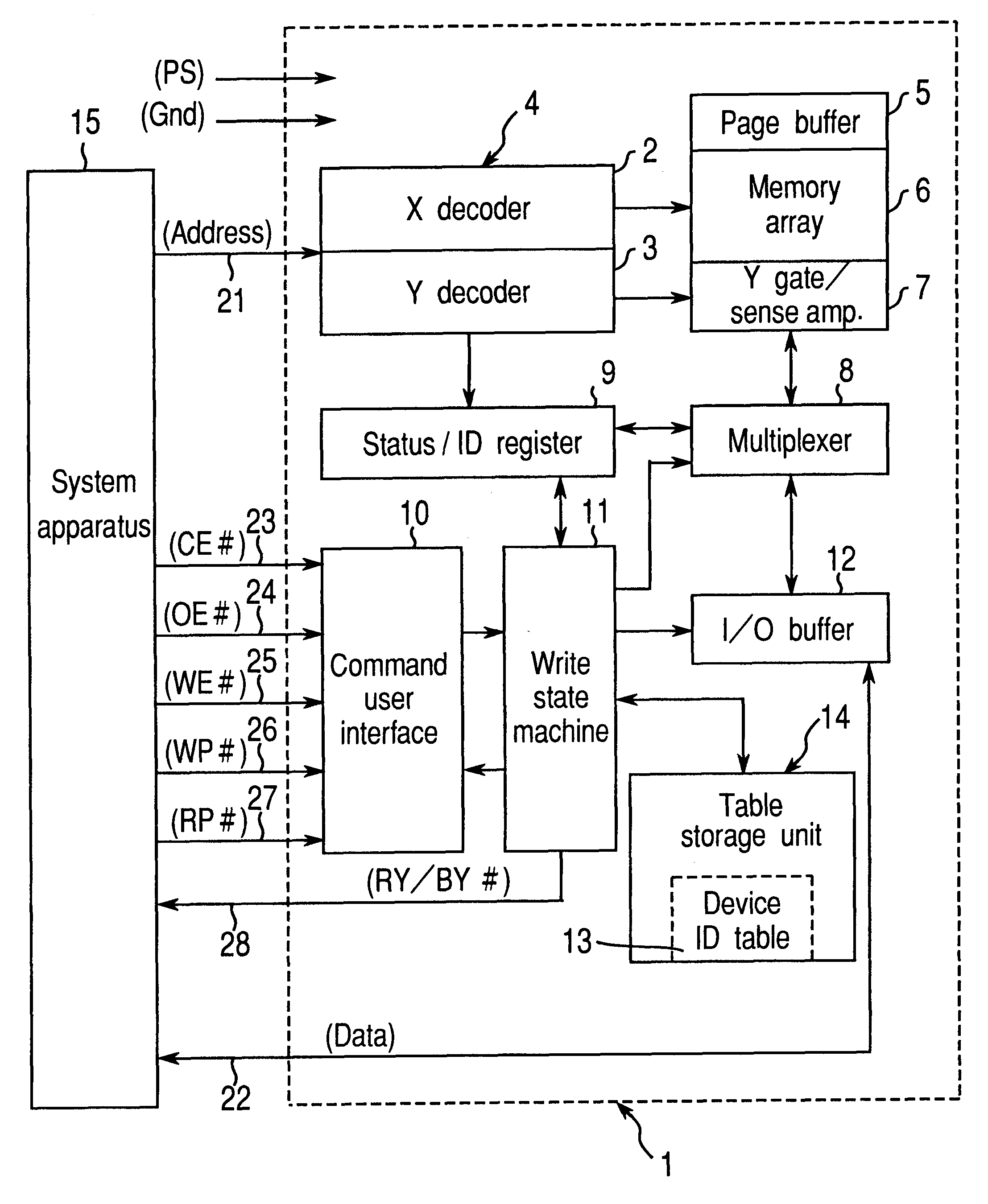
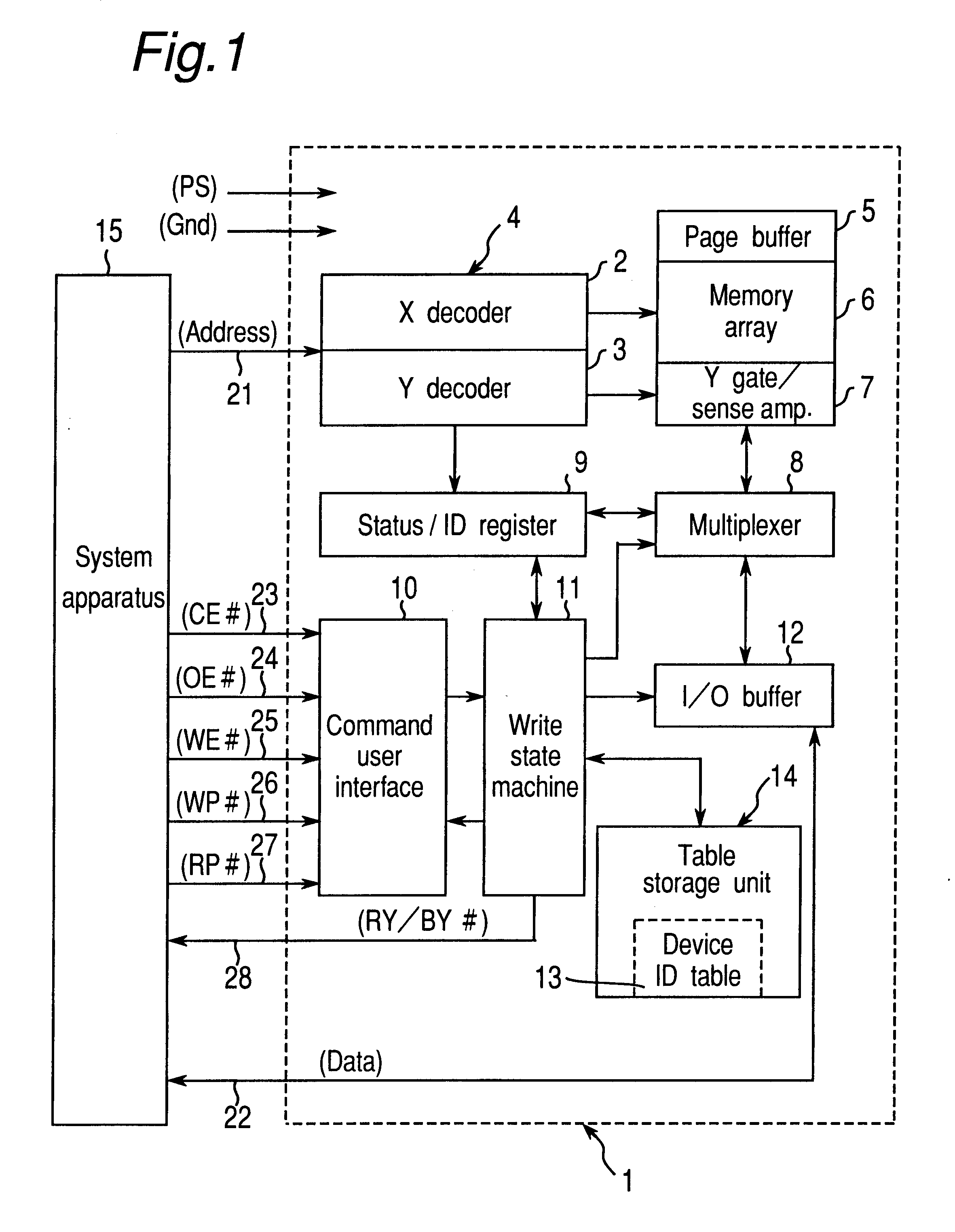
FIG. 1 is a typical block diagram of an IC memory device exemplary of a first embodiment of the present invention wherein M5M29F016 flash memory manufactured by Mitsubishi Denki Kabushiki Kaisha is used for the IC memory.
Referring to FIG. 1, the IC memory device 1 is command-controllable memory comprising an address decoder 4, a page buffer 5, memory array 6, a Y-gate sense amplifier 7, a multiplexer 8, a status / ID register 9, a command user interface (CUI) 10, a write-state machine (WSM) 11, an input / output buffer 12, and a table storage unit 14. The table storage unit 14 holds a device ID table 13. The device ID table 13 is a listing of device codes used to identify the manufacturer and device codes of compatible IC memory using the same operating algorithm.
The address decoder 4 comprises an X decoder 2 and a Y decoder 3 for decoding address data supplied from an external source. The address decoder 4 is further connected to an external host 15, which controls the IC memory device...
embodiment 2
As can be understood from the above description, the write-state machine 11 of an IC memory device 1 according to the first embodiment of the invention stores the result of the compatibility check performed by the write-state machine 11 to the status / ID register 9, and the host 15 then reads the result from the status / ID register 9. It is alternatively possible, however, to convert the check result to a predefined signal and output this signal directly to the host 15. An IC memory device 1 so comprised is described next below in connection with a second embodiment of the present invention.
It should be noted that a typical block diagram of an IC memory device according to this second embodiment is identical to that of the first embodiment shown in FIG. 1 except for the write-state machine 11 and, therefore, the IC memory device 1, which are indicated as write-state machine 31 and IC memory device 30, respectively, below. Only the differences in the IC memory device 30 of the second e...
embodiment 3
As can be understood from the preceding descriptions, the IC memory devices according to the first and second embodiments of the invention use the IC memory device for reading data only when the IC memory device is determined incompatible with the host 15. However, when the IC memory device is incompatible with the host 15, it is also possible for the IC memory device to disable itself in response to all commands from the host 15. The IC memory device so comprised is described next in connection with a third embodiment of the invention.
It should be noted that a typical block diagram of an IC memory device according to this third embodiment is identical to that of the first embodiment shown in FIG. 1 except for the write-state machine 11 and, therefore, the IC memory device 1, which are indicated as write-state machine 41 and IC memory device 40, respectively, below. Only the differences in the IC memory device 40 of the third embodiment are described below.
When the write-state machi...
PUM
 Abstract
Description
Claims
Application Information


