Substrate structure of plasma display panel and its fabricating method

a substrate structure and plasma display technology, applied in gas discharge vessels/containers, electric discharge tubes, gas-filled discharge tubes, etc., can solve the problems of low productivity, increase the unit cost of products, and improve the structur

Inactive Publication Date: 2001-04-10
LG ELECTRONICS INC
View PDF2 Cites 18 Cited by
  • Summary
  • Abstract
  • Description
  • Claims
  • Application Information

AI Technical Summary

Problems solved by technology

However, the conventional plasma display panel presents some disadvantages in that the panel whose life is at most about 5,000 hours needs a structural improvement to secure long life more than 30,000 hours.
Moreover, the protection layer is generally formed by E-beam deposition and such formation by E-beam deposition results in low productivity because of the need for complicated process such as vacuum and heat treatments and the expensive equipment required therefor, thus raising the unit cost of products.

Method used


Image

  • Substrate structure of plasma display panel and its fabricating method
  • Substrate structure of plasma display panel and its fabricating method
  • Substrate structure of plasma display panel and its fabricating method

Examples


first embodiment

the present invention as constructed above is formed in the following method.

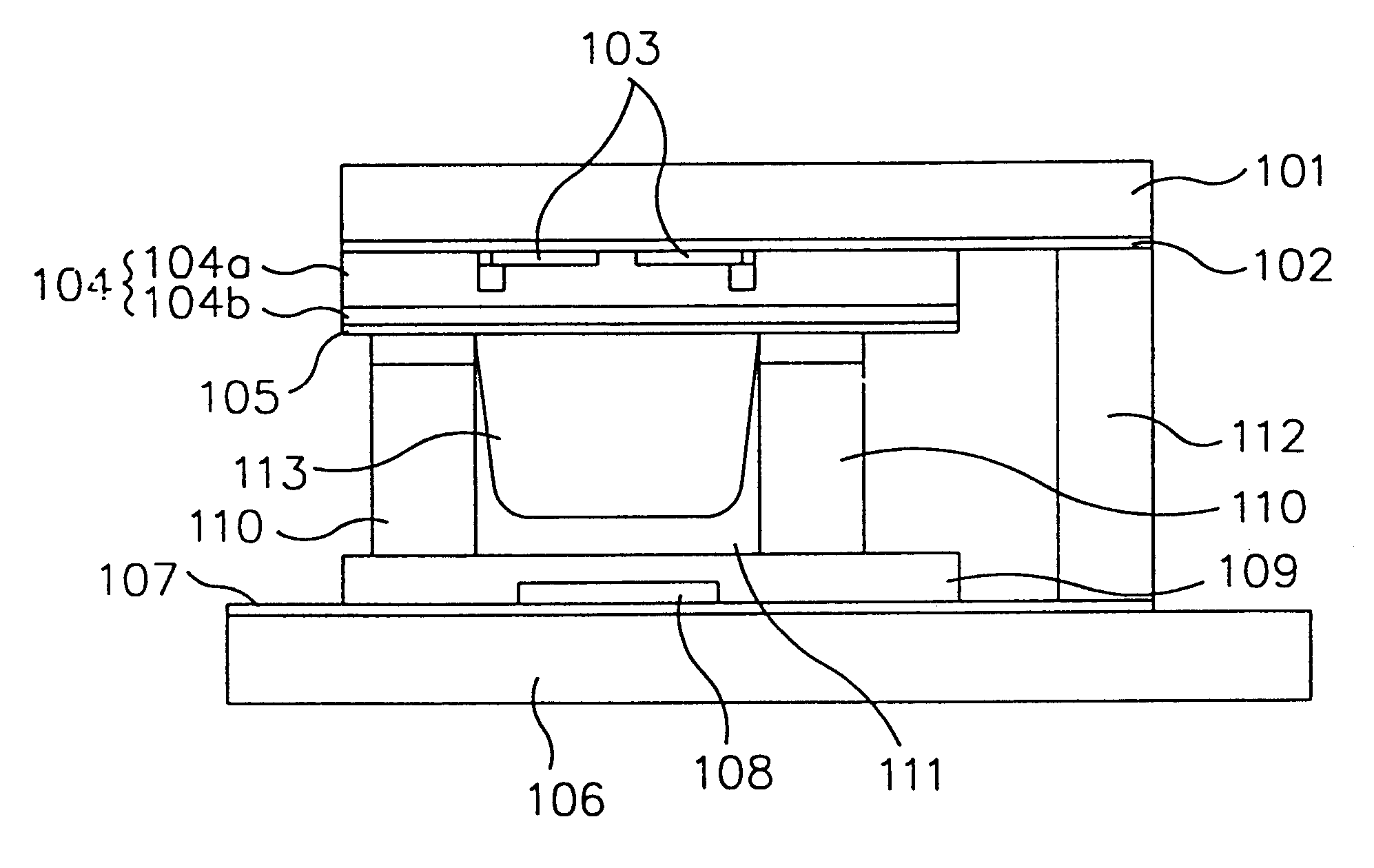
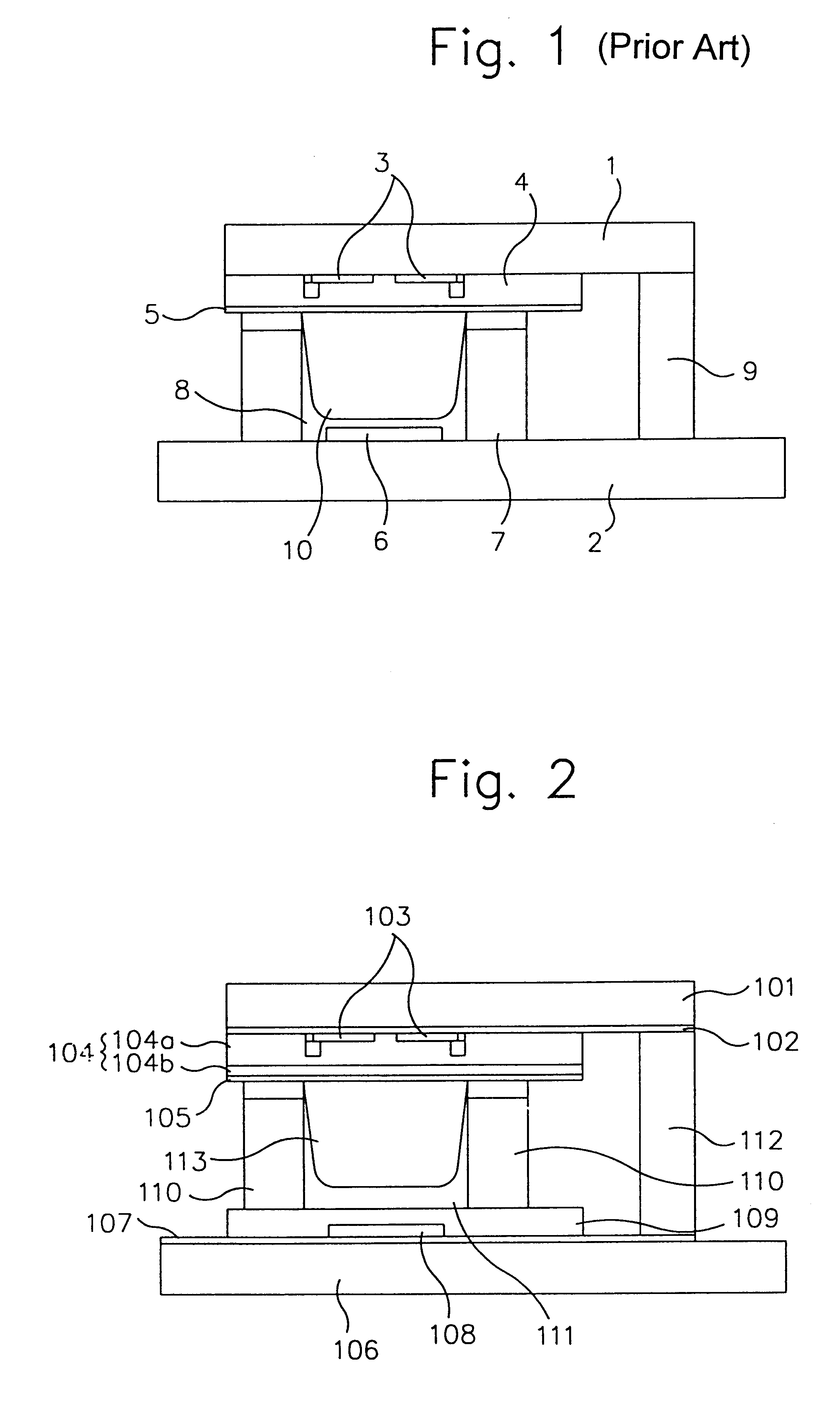
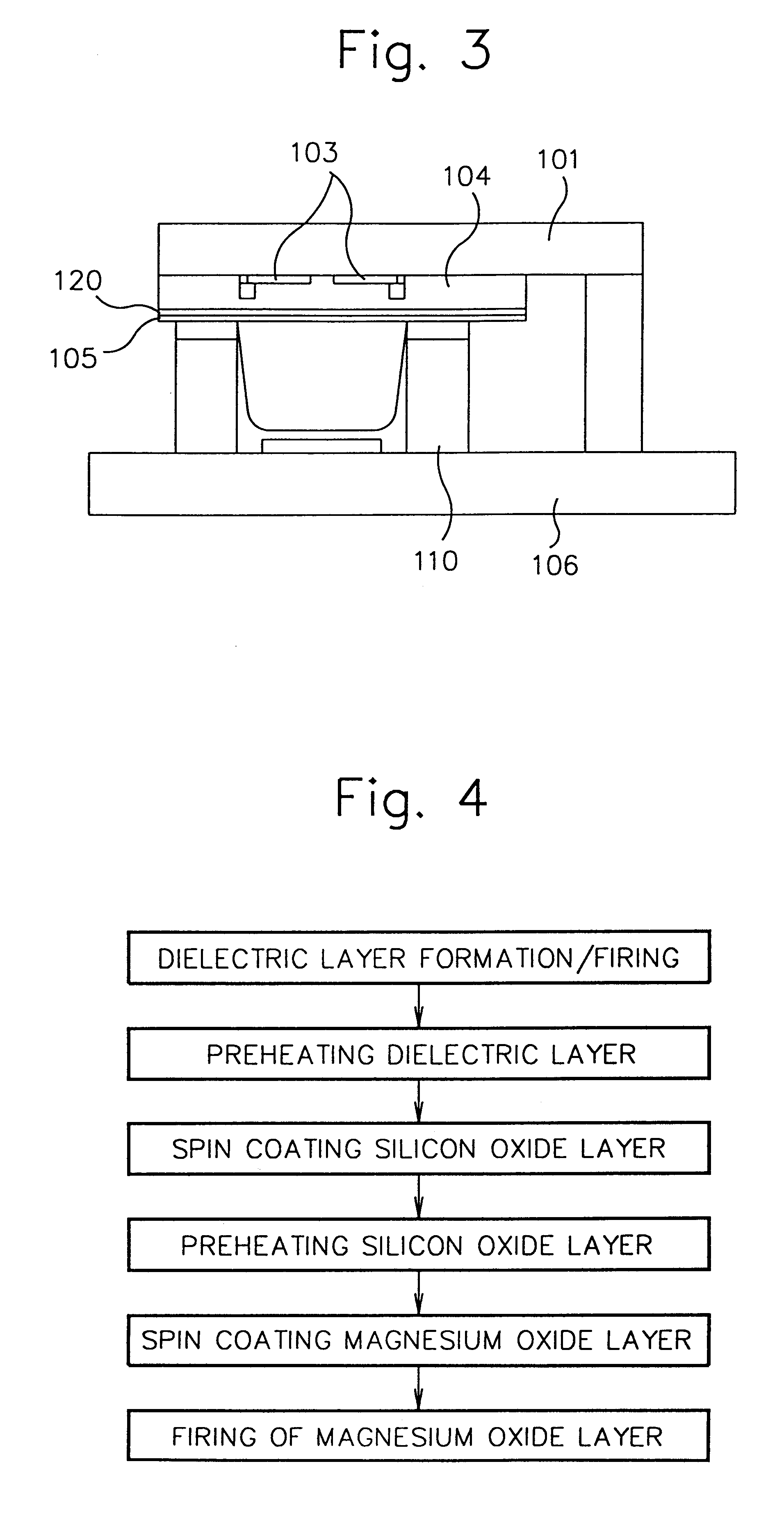
Upper and lower structures are first formed by a separate process. To form the upper structure, silicon oxide is deposited on the upper surface of the upper substrate 101 to form the first transparent, underlayer 102 in the 20 to 90 nm range of thickness, in a simplified process, by either dipping or spin coating method.

The upper electrodes 103 are then formed on the first underlayer 102. Each upper electrode includes a transparent electrode and a metal electrode narrower than the transparent electrode, where the metal electrode is in contact with the transparent electrode. The metal electrode may be made of aluminum or black pigment-added aluminum. On the first underlayer 102 is formed the upper dielectric layer 104 which drops the driving voltage by generating wall charges. The upper dielectric layer 104 comprises a first dielectric layer 104a having high voltage-resistance, and a second dielectric layer ...


PUM


Abstract

An electrode structure of a PDP (plasma display panel) and its manufacturing method, where the production cost is curtailed with the extension of life by forming a protection layer of excellent properties and low cost on an insulating substrate during the manufacture of the panel. The structure comprises two substrates coupled in parallel with each other by frit glass. One of the two substrates has sustain electrodes. One or more dielectric layers are formed over the sustain electrodes, and an interfacial reaction preventive layer and a protection layer are formed over the dielectric layers. The other substrate has address electrodes arranged thereon. A lower dielectric layer is formed over the address electrodes. Barriers coated with phosphor are formed between the upper and lower substrates. The protection layer may be deposited in a multilayered form by a spin coating method.

Description

A. Field of the InventionThe present invention relates to a PDP (Plasma Display Panel) and, more particularly, to a PDP substrate structure and its fabricating method.B. Description of the Prior ArtA general color PDP, as shown in FIG. 1, has upper and lower structures. The upper structure comprises an upper substrate 1, a sustain electrode 3 formed on the upper substrate, a dielectric layer 4 for maintaining the surface charge generated during a discharge of the sustain electrode 3, and a protection layer 5. The lower structure comprises a lower substrate 2, and an address electrode 6 formed on the lower substrate 2. Barriers 7 coated with phosphor 8 are formed between the upper and lower substrates 1 and 2. A frit glass 9 is formed at the glass end portion, combining the upper and lower substrates 1 and 2.Reference numeral 10 indicates a discharging gas sealed in a space between the upper and lower structures.It is considered that the PDPs are the most suitable flat display device...

Claims


Application Information

Patent Timeline
Patent Type & Authority Patents(United States)
IPC IPC(8): H01J17/49H01J11/12H01J11/38
CPCH01J11/12H01J11/38
Inventor KIM, GUN-WOOKIM, JIN-YOUNG
Owner LG ELECTRONICS INC
Why Eureka
Try Eureka