Embedded LSI having a FeRAM section and a logic circuit section

Inactive Publication Date: 2001-04-17
RENESAS ELECTRONICS CORP
View PDF2 Cites 57 Cited by
  • Summary
  • Abstract
  • Description
  • Claims
  • Application Information

AI Technical Summary

Problems solved by technology

The desorption of oxygen damages the ferroelectric film of the ferroelectric capacitor and thus degrades characteristics of the ferroelectric capacitor, which is undesirable
This is because these CVD steps also generate hydrogen similarly to the hydrogen-annealing step, a

Method used


Image

  • Embedded LSI having a FeRAM section and a logic circuit section
  • Embedded LSI having a FeRAM section and a logic circuit section
  • Embedded LSI having a FeRAM section and a logic circuit section

Examples


first embodiment

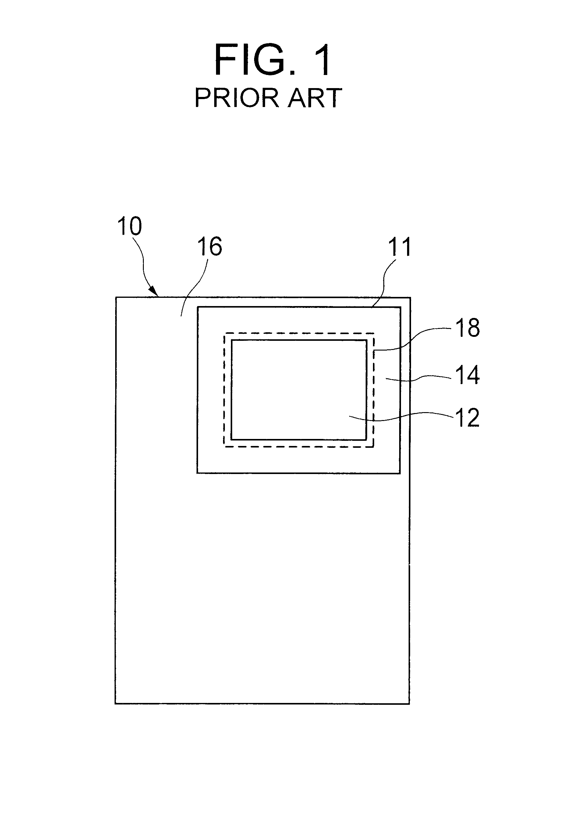
Referring to FIG. 3, an embedded LSI according to the present invention is shown as a chip in a wafer. The LSI 40 includes a logic circuit section 42 and a FeRAM macro block 41 having a central FeRAM cell array 44 and a peripheral circuit 45 for controlling the FeRAM cell array 44. The logic circuit section 42 includes therein a microcomputer, a plurality of controllers, a SRAM, input / output interfaces and input / output pads which are not explicitly shown in the figure. The embedded LSI 40 is separated by a scribing area 43 from other embedded LSIs. The entire area for the FeRAM macro block 41 is covered by a hydrogen barrier layer 80 as shown by hatching.

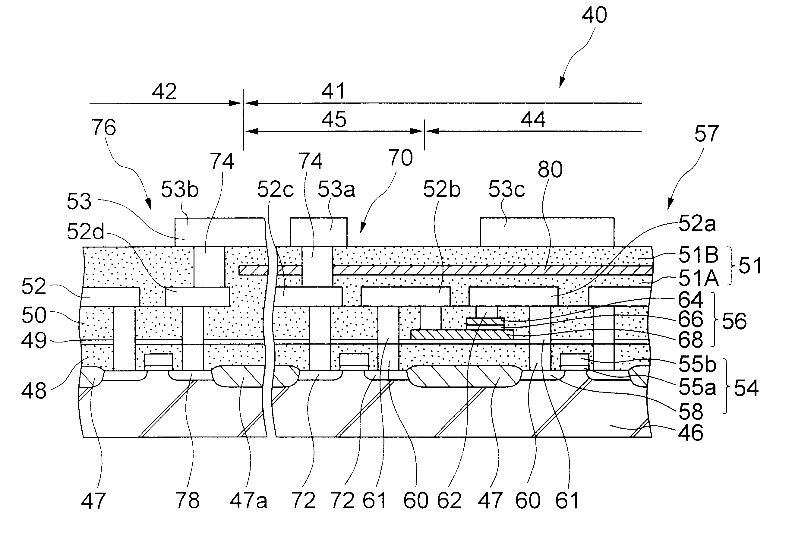
Referring to FIG. 4 showing a sectional view of the embedded LSI 40 of FIG. 3, the logic circuit section 42, the peripheral circuit 45 and the FeRAM cell array 44 are separated from one another by isolation films 47 (including 47a) formed on a silicon substrate 46.

The embedded LSI 40 has a laminated insulation structure including a ...

third embodiment

Referring to FIG. 9, an embedded LSI 110 according to the present invention includes a FeRAM macro block 41 at a corner region of the chip where two elongate scribing areas 43 intersect one another. The peripheral circuit 45 of the FeRAM macro block 41 is disposed at the boundary between the logic circuit section 42 and the FeRAM macro block, and not disposed in the periphery of the chip.

In the embedded LSI of FIG. 9, the hydrogen barrier layer 80 shown by hatching covers the FeRAM cell array 41, the peripheral circuit 45 and portions 43A and 43B of the scribing area 43 adjacent to the FeRAM macro block 41. The hydrogen barrier layer 80 covering the portions 43A and 43B of the scribing area 43 effectively prevents hydrogen from entering the FeRAM macro block 41 during the ale hydrogen-annealing process. The peripheral circuit 45 disposed at the boundary between the FeRAM macro block 41 and the logic circuit section 42 also effectively prevents the hydrogen from entering the FeRAM ma...

fourth embodiment

Referring to FIG. 10, an embedded LSI 120 according to the present invention has a FeRAM macro block 41 in the vicinity of a scribing area 43 of a wafer. The peripheral circuit 45 of the FERAM macro block 41 is disposed at three sides 122A, 122B and 122C of the FeRAM macro block 41 constituting the boundary between the FeRAM macro block 41 and the logic circuit section 42. The hydrogen barrier layer 80 shown by hatching covers the FeRAM cell array 41, the peripheral circuit 45 and a portion 43C of the scribing area 43 adjacent to the FeRAM macro block 41.

The hydrogen barrier layer 80 covering the portion 43C of the scribing area 43 and the peripheral circuit 45 effectively prevents the ingress of hydrogen.

In the first and second embodiments, the hydrogen barrier layers 80 and 106 are implemented by 100-nm-thick plasma CVD Si.sub.3 N.sub.4. The plasma CVD Si.sub.3 N.sub.4 may be replaced by other films, the configurations of which are tabulated in following Table 1.

In addition, in th...


PUM


Abstract

An embedded LSI includes a FeRAM macro block and an associated logic circuit section. A hydrogen barrier layer covers the FeRAM macro block as a whole and exposes the logic circuit section. The edge of the hydrogen barrier layer overlies the peripheral circuit of the FeRAM macro block and the boundary separating the FeRAM macro block from the logic circuit section. The ferroelectric capacitor is protected by the hydrogen barrier layer against hydrogen during a hydrogen-annealing process.

Description

(a) Field of the InventionThe present invention relates to an embedded LSI and, more particularly, to an embedded LSI having a FeRAM section and a logic circuit section.(b) Description of the Related ArtRecently, IC cards each having a nonvolatile memory device and a logic circuit embedded on a single substrate are expected to replace conventional magnetic cards. The nonvolatile memory device in the IC card generally includes a memory cell array and an associated peripheral circuit including a drive section and a decoder section, whereas the logic circuit includes a processing section for conducting data processing and an input / output section for conducting input / output processing in association with the peripheral circuit and the memory cell array.With the increase in the amount of data to be stored in the memory cell array, a conventional EEPROM used as the nonvolatile memory device will be rapidly replaced by a FeRAM which has a larger storage capacity with high speed operation a...

Claims


Application Information

Patent Timeline
IPC IPC(8): H01L21/70H01L21/8246H01L27/105H01L21/822H01L27/04H01L27/10
CPCH01L27/105H01L27/11502H01L27/11507H01L27/11509H10B53/40H10B53/30H10B53/00H01L27/10
Inventor KASAI, NAOKI
Owner RENESAS ELECTRONICS CORP
Why Eureka
Try Eureka