Manufacturing technology of gate dielectric layer of silicon carbide semiconductor device

A gate dielectric layer and manufacturing process technology, applied in the field of gate dielectric layer manufacturing process, can solve the problems of unsatisfactory passivation and reduced interface state density, etc.

Inactive Publication Date: 2017-04-19
NANJING LISHENG SEMICON SCI & TECH CO LTD
View PDF4 Cites 12 Cited by
  • Summary
  • Abstract
  • Description
  • Claims
  • Application Information

AI Technical Summary

Problems solved by technology

[0022] In general, hydrogen passivation, nitrogen passivation and phosphorus passivation, or the mixed passivation among them, can reduce the interface state density and thus increase the channel mobility, but compared with the Si-SiO2 channel mobility, the above The passivation is still not ideal, the present invention proposes other passivation methods, it is believed that the mobility can be further improved to higher than 100cm2 / V-s

Method used


Image

  • Manufacturing technology of gate dielectric layer of silicon carbide semiconductor device
  • Manufacturing technology of gate dielectric layer of silicon carbide semiconductor device
  • Manufacturing technology of gate dielectric layer of silicon carbide semiconductor device

Examples


Embodiment

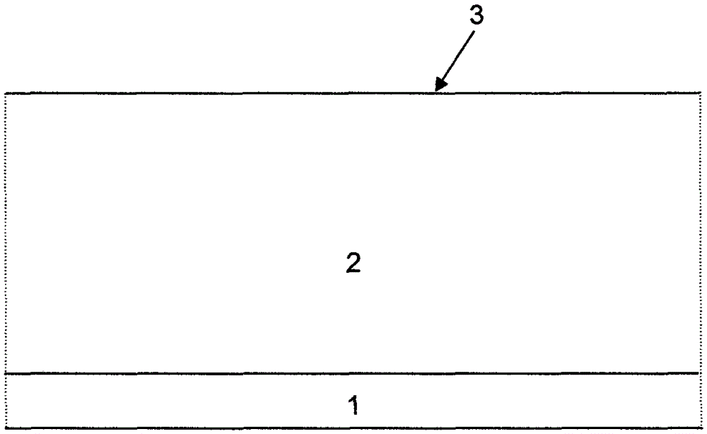
[0063] Such as figure 1 As shown, the silicon carbide surface is cleaned first, and the oxygen atoms on the silicon carbide surface are removed before depositing the dielectric layer, leaving a surface dominated by silicon atoms.

[0064] Such as figure 2 As shown, a layer of silicon nitride is deposited on the surface of silicon carbide by atomic layer deposition or molecular beam epitaxy.

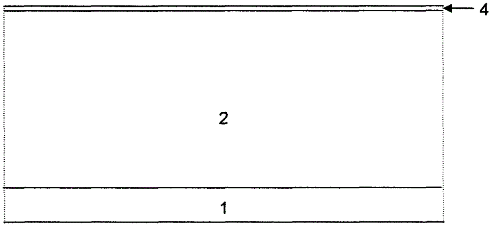
[0065] Such as image 3 As shown, a layer of silicon is deposited on a silicon nitride layer by atomic layer deposition or molecular beam epitaxy.

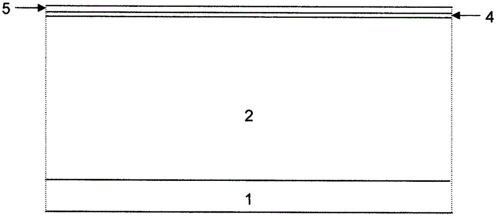
[0066] Such as Figure 4 As shown, a layer of polysilicon or amorphous silicon is then deposited by CVD.

[0067] Such as Figure 5 As shown, then all the silicon above the silicon nitride layer is oxidized by thermal oxidation, and the oxide layer and the silicon nitride layer together form a gate dielectric layer.

[0068] After the oxide layer is formed, various high-temperature annealing such as hydrogen annealing, nitrogen anneali...


PUM


Abstract

The invention relates to a manufacturing technology of a gate dielectric layer of a silicon carbide semiconductor device. The technology comprises the following steps of cleaning a silicon carbide surface, before a dielectric layer is deposited, removing oxygen atoms of the silicon carbide surface so that the surface taking silicon atoms as a main component is remained; using an atomic layer deposition method or a molecular beam epitaxy method to deposit a layer of silicon nitride (SiN) on the silicon carbide surface; then using the atomic layer deposition method or the molecular beam epitaxy method to deposit a layer of silicon; and using a CVD method to deposit a layer of polycrystalline silicon or amorphous silicon; and then using a thermal oxidation method to oxidize all the silicon above the SiN layer, wherein an oxidation layer and a silicon nitride layer commonly form the gate dielectric layer; and after the oxidation layer is formed, carrying out various kinds of high temperature annealing, such as hydrogen annealing, nitrogen annealing, phosphorus annealing, or annealing of various combinations of hydrogen+nitrogen+phosphorus and the like.

Description

technical field [0001] The invention relates to a manufacturing process of a gate dielectric layer of a silicon carbide device, in particular to a manufacturing method for a silicon carbide semiconductor device using a dielectric layer plus a silicon dioxide layer as a gate dielectric layer. Background technique [0002] Most traditional integrated circuits using silicon devices can only work below 250°C, which cannot meet the requirements of high temperature, high power and high frequency. Among them, the new semiconductor material silicon carbide (SiC) has attracted the most attention and research. [0003] Silicon carbide semiconductor materials have outstanding advantages such as wide band gap, high saturation drift velocity, high thermal conductivity, and high critical breakdown electric field, and are especially suitable for the production of high-power, high-voltage, high-temperature, and radiation-resistant electronic devices. [0004] Silicon carbide has a wide ban...

Claims


Application Information

Patent Timeline
Patent Type & Authority Applications(China)
IPC IPC(8): H01L21/336H01L21/331H01L21/28H01L21/285
CPCH01L21/28008H01L21/285H01L29/66068
Inventor 苏冠创黄升晖
Owner NANJING LISHENG SEMICON SCI & TECH CO LTD
Why Eureka
Try Eureka