Memory having user programmable AC timings

a programmable ac timing and memory technology, applied in the field of memory devices, can solve the problems of exacerbated challenges, data integrity of data-valid windows poses a significant challenge, and static ram provides faster access to data but is more expensive than dram

Inactive Publication Date: 2001-04-17
IBM CORP
View PDF8 Cites 97 Cited by
  • Summary
  • Abstract
  • Description
  • Claims
  • Application Information

AI Technical Summary

Problems solved by technology

Static RAM provides faster access to data but is more expensive than DRAM.
The integrity of data-valid windows poses a significant challenge for high-frequency input/output (I/O) interfaces.
This challenge is exacerbated by the fact that the timing of the SRAM chip standing alone may be effected somewhat at the system level (i.e., once the SRAM is integrated as part of an actual cache system the timing requirements may change).
Data

Method used


Image

  • Memory having user programmable AC timings
  • Memory having user programmable AC timings
  • Memory having user programmable AC timings

Examples


Embodiment Construction

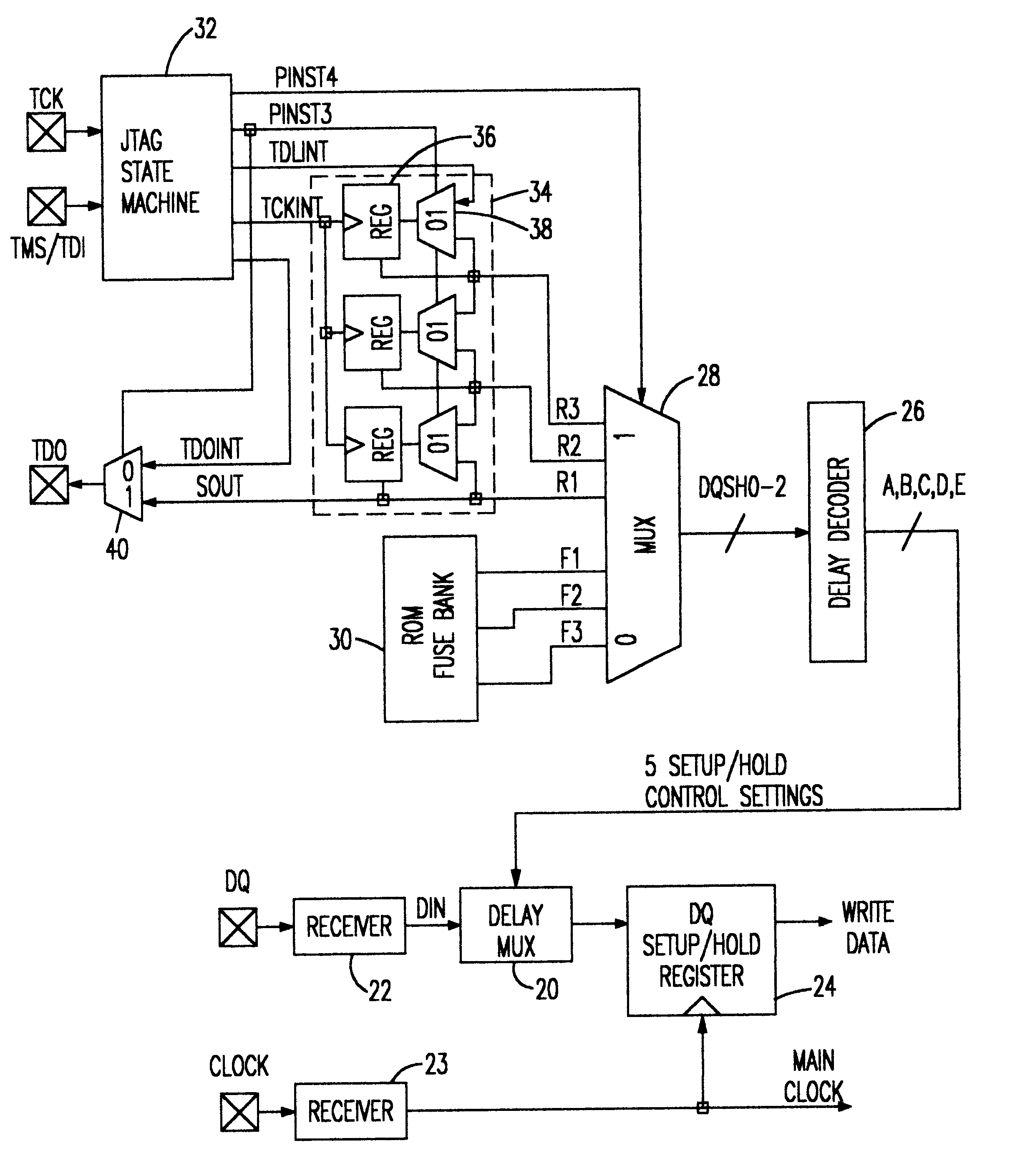
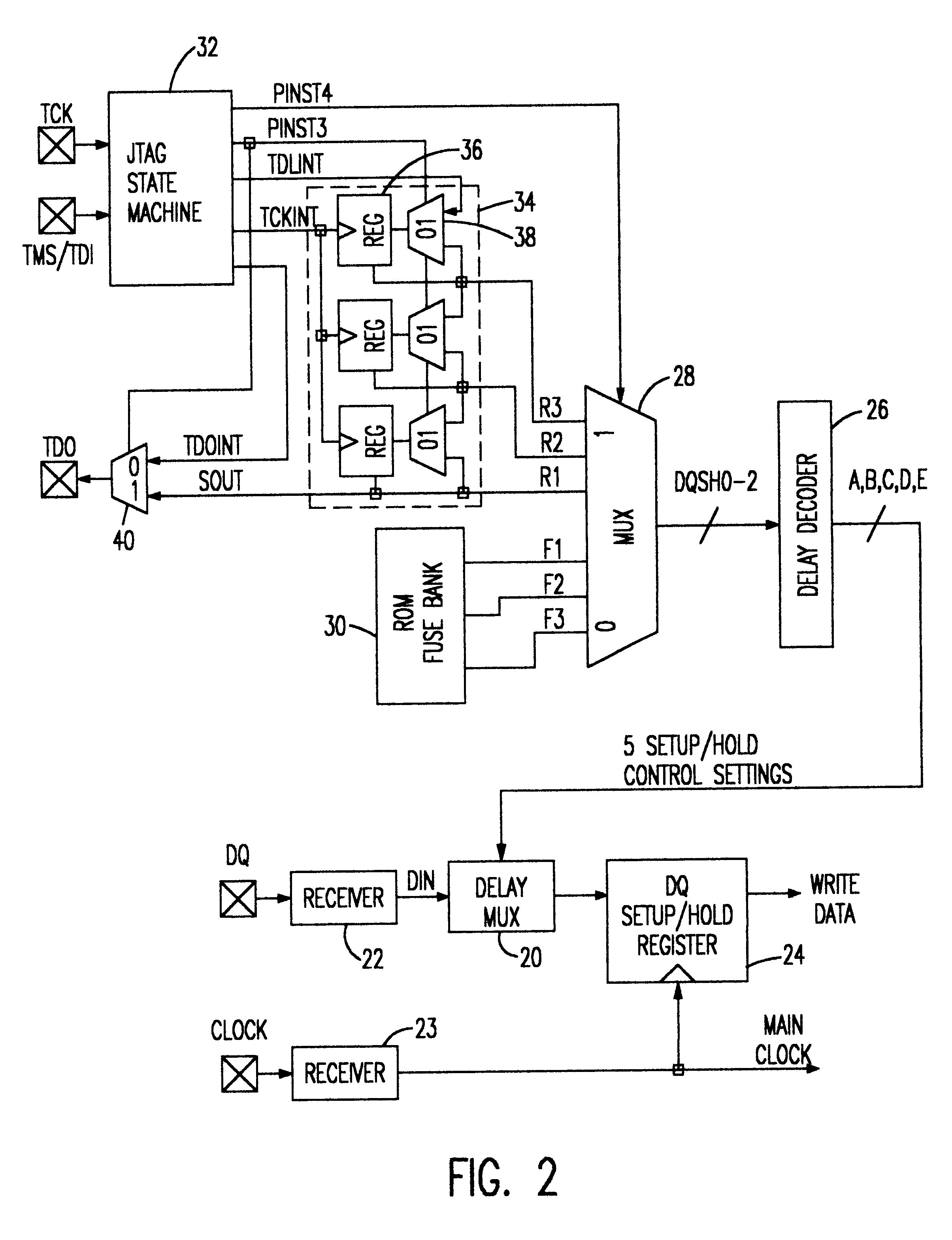
Referring now to the drawings, and more particularly to FIG. 2, there is shown the relevant portions of the SRAM module according to the present invention. A delay circuit 20 is placed in a path between data input pin DQ and receiver 22 and the DQ set-up and hold register 24. The register circuit is clocked by the main system clock input through the receiver 23.

For simplicity of illustration, the delay circuit 20 is shown on the data input side (write) of the SRAM. However, it is to be understood that the teachings of the present invention are also applicable to adjusting the AC timings of either data or address pins on both the input side (write) or output side (read) of the SRAM.

A delay decoder 26 outputs one of a plurality of signals that instructs the delay circuit 20 by how much to advance or retard the AC timing of the particular DQ pin. A multiplexer (MUX) circuit 28 inputs a timing program into the delay decoder 26. This timing program originates from one of two places.

The f...


PUM


Abstract

A SRAM module provides programmability of AC timings such that an end user can adjust or "tweak" the AC timings to maximize system performance. A variable delay circuit is placed in the path between a signal (e.g., data signal or address signal)and the SRAM set-up and hold register which allows the user to shift the setup-and-hold window by selected increments. The delay circuit can either advance or retard the AC timings. A delay program controlling the delay circuit is selected in one of two ways; either by a default AC timing program stored in a ROM device and preset by the manufacturer, or by a private JTAG instruction and AC programming data input by the user through the JTAG state machine provided on the SRAM chip. Once the optimum delay (or advance) is selected to optimize the SRAM to the cache system this user program may be permanently burned into the default ROM such that the optimum timings are used thereafter as the default.

Description

1. Field of the InventionThe present invention generally relates to memory device that has user programmable alternating current (AC) timings and, more particularly, to a programmable SRAM memory which uses either default timing specifications stored in a fuse bank or allows the user to customize the timing specifications of individual pins via a JTAG instruction.2. Description of the Related ArtStatic random access memory (SRAM) is a type of high speed memory wherein each bit is represented by the state of a circuit with two stable states. Such a "bistable" circuit can be built with four transistors (for maximum density) or six (for highest speed and lowest power). SRAM retains data bits in its memory as long as power is being supplied. Unlike dynamic RAM (DRAM), which stores bits in cells made up of a capacitor and a transistor, SRAM does not have to be periodically refreshed. Static RAM provides faster access to data but is more expensive than DRAM. SRAM is commonly used for a co...

Claims


Application Information

Patent Timeline
IPC IPC(8): G11C7/00G11C7/22G11C7/10G11C11/417
CPCG11C7/1045G11C7/22G11C11/417
Inventor BRACERAS, GEORDIE M.LAMPHIER, STEVEN H.PILO, HAROLD
Owner IBM CORP
Why Eureka
Try Eureka