

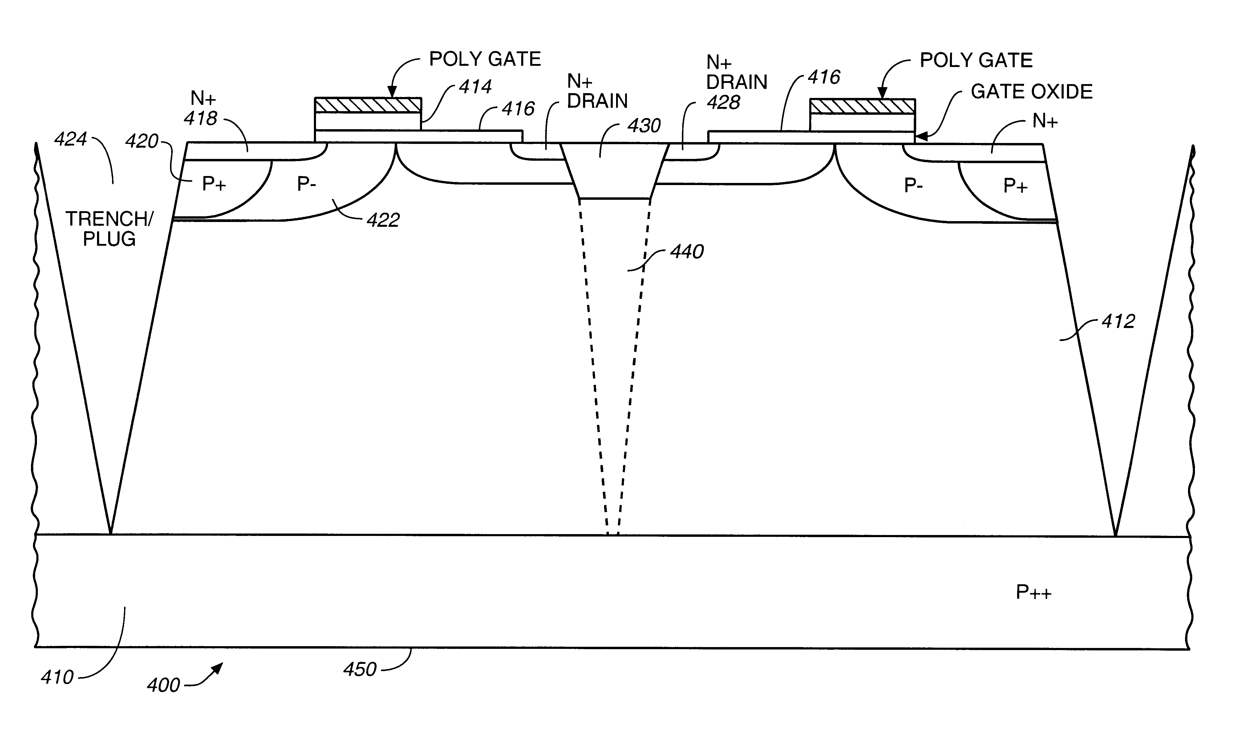
Lateral RF MOS device with improved drain structure
a technology of lateral rf mos and drain structure, which is applied in the manufacture of semiconductor/solid-state devices, semiconductor devices, electrical apparatus, etc., can solve the problems of insufficient maximum current flow density of prior art lateral rf mos devices in the source-drain channel, limited source-drain channel dimensions, and inability to use prior art lateral rf mos devices as power amplifiers with sufficient bandwidth
- Summary
- Abstract
- Description
- Claims
- Application Information
AI Technical Summary
Problems solved by technology
Method used
Image

Examples
Embodiment Construction
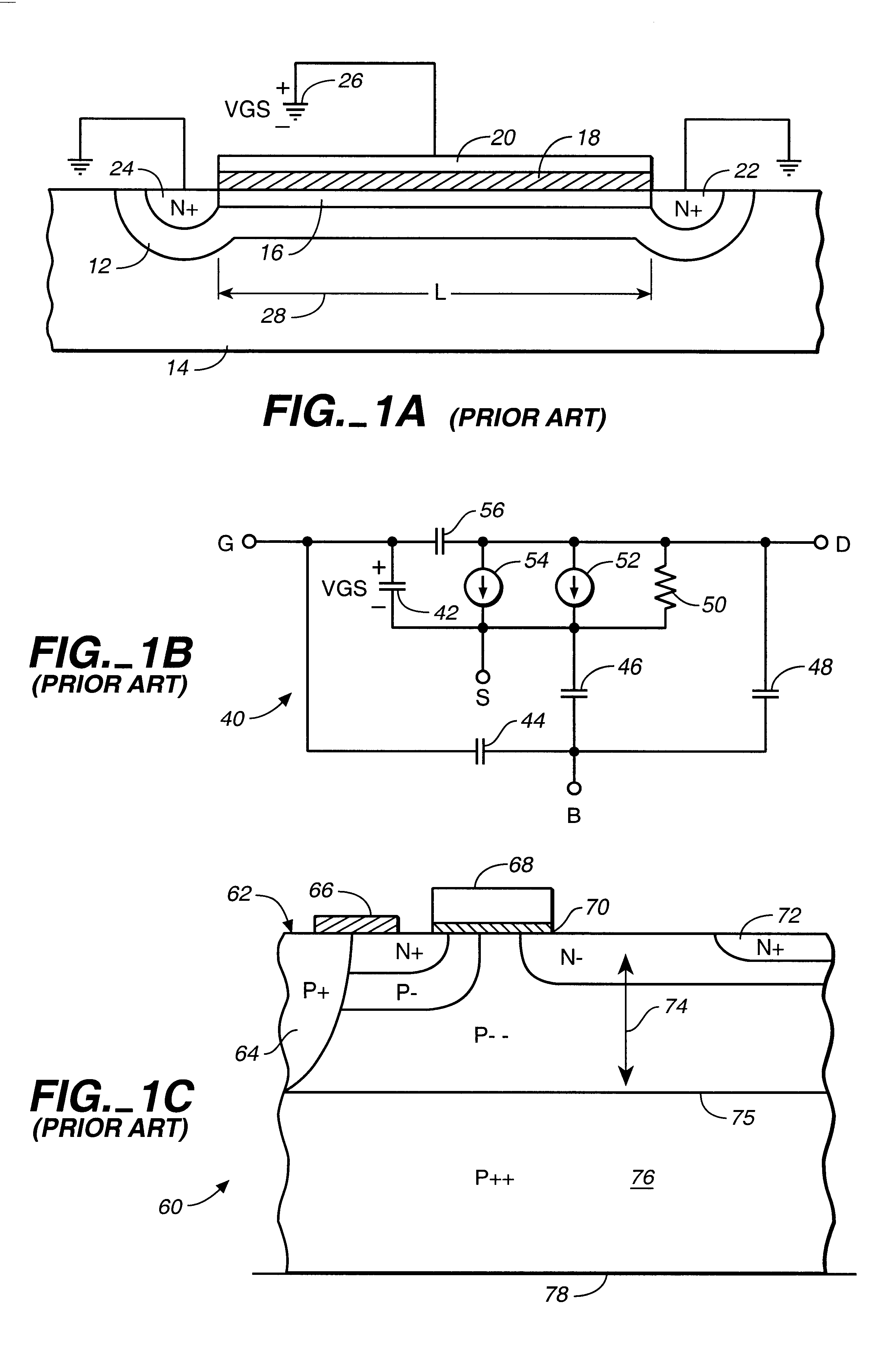
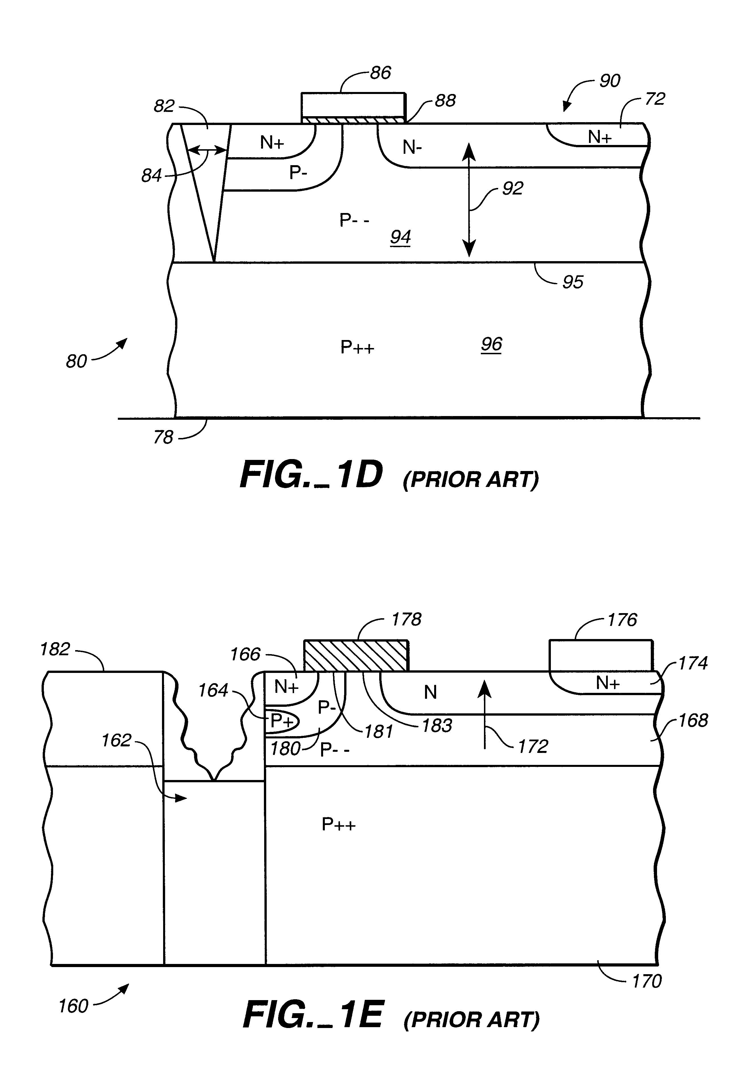
An idealized NMOS device cross section with depletion and induced channel and with applied positive VG.sub.GS is shown in FIG. 1A. For the complete reference, please, see "Analysis and Design of Analog Integrated Circuits" by Paul Gray and Robert Meyer, published by John Wiley & Sons, Inc., 1993.
In the large-signal model of a typical NMOS device, we consider substrate, source, and drain grounded and a positive voltage V.sub.GS (between the gate (20) and the substrate (14)) applied to the gate as shown in FIG. 1A. The gate and the substrate form the plates of a capacitor with the layer of silicon oxide (SiO.sub.2) (18) as a dielectric. Positive charge accumulates on the gate and negative charge in the substrate. Initially, the negative charge in the P-type substrate is manifested by creation of a depletion region (12) and resulting exclusion of holes under the gate. The depletion-layer width X under the oxide is:
X=(2.di-elect cons..phi. / qN.sub.A).sup.1 / 2 ; (1)
where .phi. is the poten...
PUM
 Abstract
Description
Claims
Application Information