High efficiency power amplifier

a power amplifier, high-efficiency technology, applied in the direction of electric variable regulation, process and machine control, instruments, etc., can solve the problems of high duty cycle, inapplicability of "class c" operation, and power need

a power amplifier, high-efficiency technology, applied in the direction of electric variable regulation, process and machine control, instruments, etc., can solve the problems of high duty cycle, inapplicability of "class c" operation, and power need

US6236273B1Inactive Publication Date: 2001-05-22SYNAPTICS INC

Image

  • High efficiency power amplifier
  • High efficiency power amplifier
  • High efficiency power amplifier

Examples


Embodiment Construction

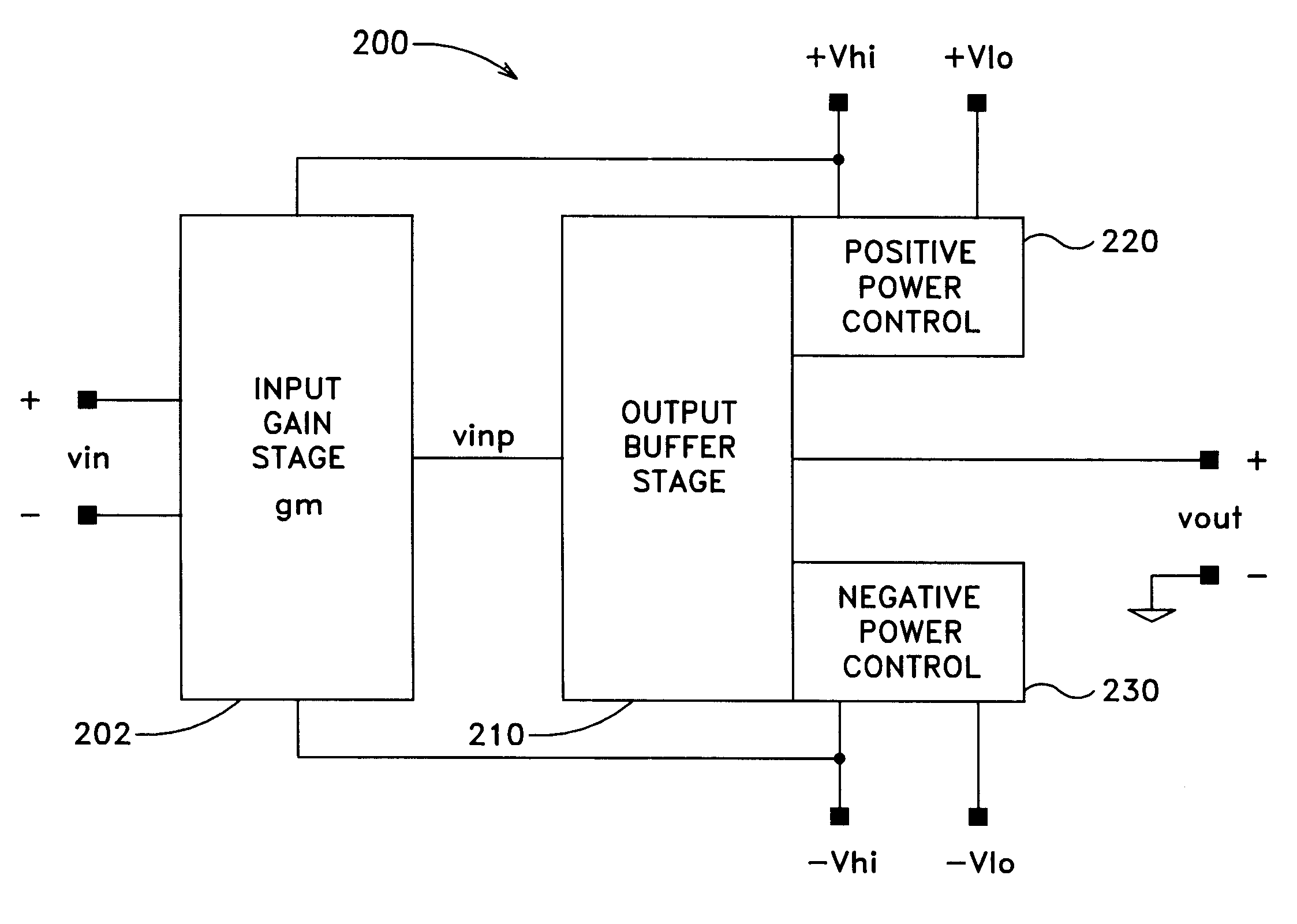
FIG. 3 is a block diagram illustrating the preferred embodiment of the invention, with the buffer stage within the block 210, and the positive and negative power control circuits within blocks 220 and 230, respectively. In FIG. 3, conventional monolithic, bipolar NPN and PNP transistors are indicated with reference designations as Nk and Pk, respectively, (k=1, 2, . . . ). Conventional current sources and resistors are similarly indicated as ik and Rk, respectively, (k=1, 2, . . . ).

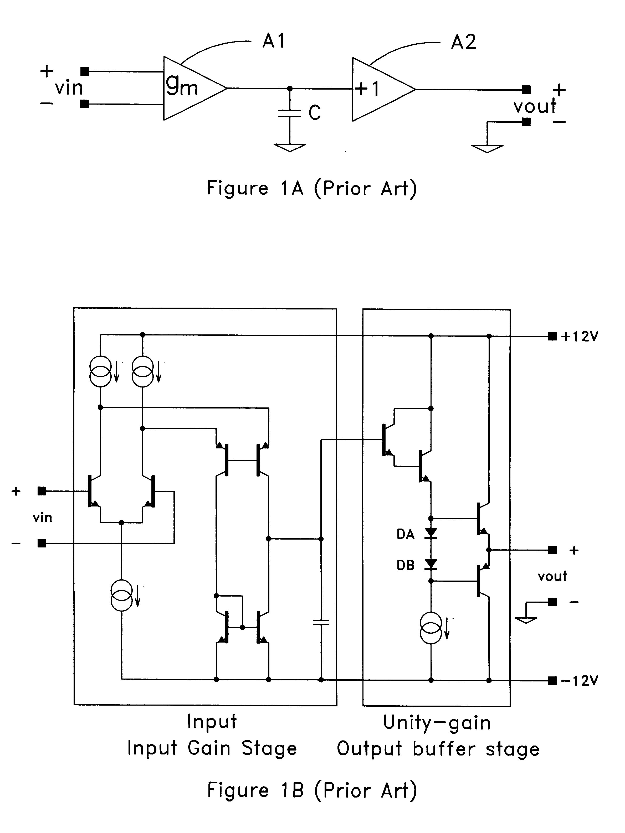
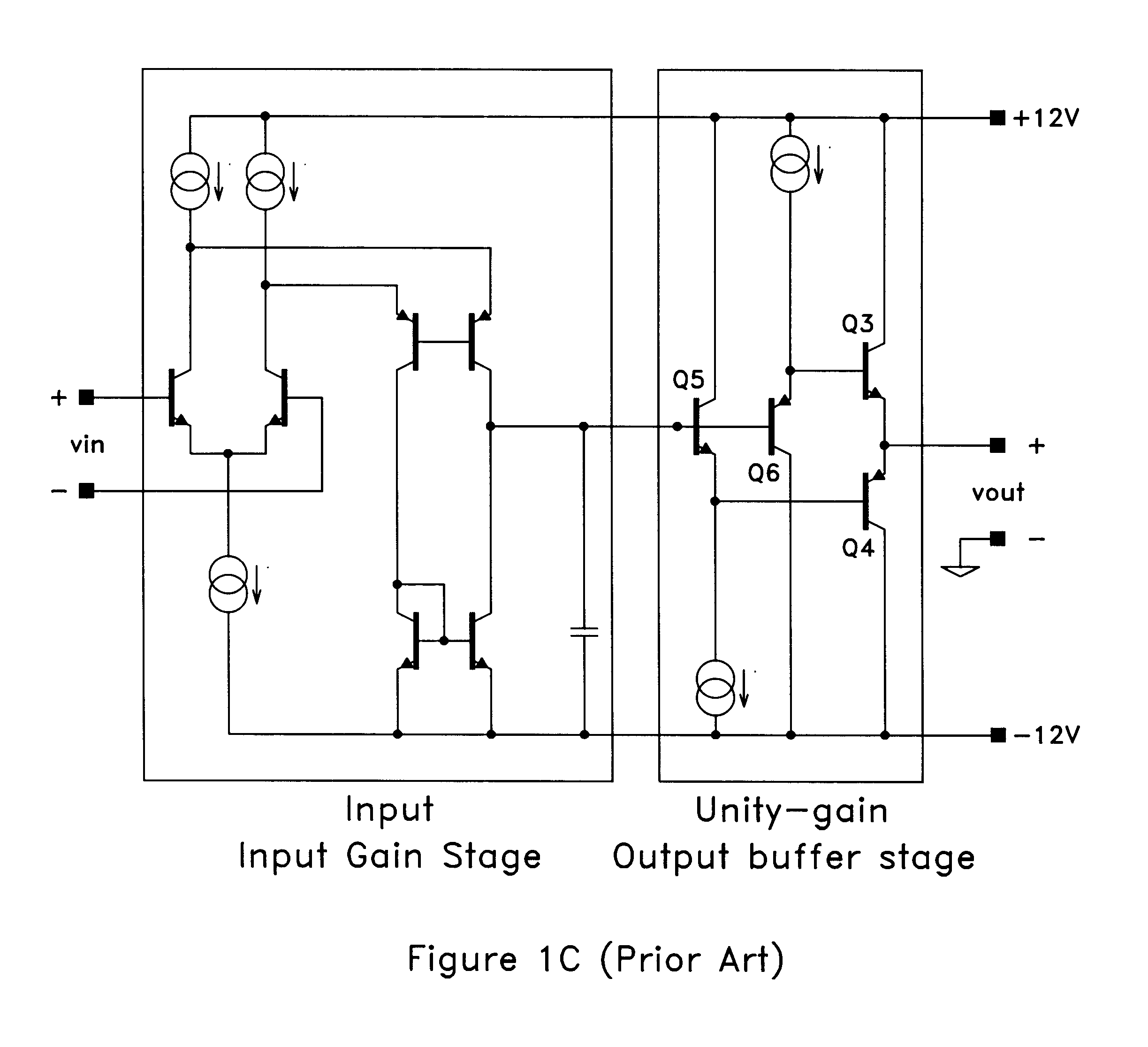
As is well known, the voltage drop (or rise) over a standard PN junction is roughly 600-800 mV, depending on operating parameters such as temperature (and thus on how much current is passing through the junction). All of the transistors used in the preferred embodiment of the invention are preferably fabricated on the same substrate, so that the voltage drop over any junction can be assumed to be nearly the same in magnitude as that over any other junction operating at approximately the same current dens...


PUM


Abstract

A monolithic integrated circuit amplifier has a gain stage and a buffer stage. The buffer stage includes an output stage and two separate voltage supplies, the second of which has a greater magnitude than the first. Switching circuitry is included that is connected to the output stage via a regulator bus. When an output demand voltage is less than a switch-over threshold, current to the output stage is provided substantially entirely from the first voltage supply; when the output demand voltage is greater than the switch-over threshold, current to the output stage is provided substantially entirely from the second voltage supply. Collector voltage at the output stage can be maintained greater than the emitter voltage by a predetermined, substantially constant amount. Voltage headroom circuitry is preferably also included for setting a voltage headroom, that is, the lowest voltage constantly available at the second current terminal of the output transistor relative to the first current terminal of the output transistor.

Description

1. Field of the InventionThis invention relates to power amplifiers and more particularly to high-power, monolithic, integrated circuit (IC) power amplifiers.2. Background ArtCertain telecommunications standards have been developed in the United States to provide high-speed digital access between customers and a central office. One example is the Asymmetric Digital Subscriber Loop (ADSL) standard, which provides a data rate of approximately 6 Mb in the direction from the central telephone office to the customer. As a result of the high data rate, ADSL has become one of the preferred standards for supplying, for example, Internet service over a standard copper wire twisted pair.Although it offers a high data rate, the ADSL standard requires that the line-driving amplifier at the central office be able to supply a signal of approximately 20 dBm (power with respect to a reference level of 1 mW) in power with a peak-to-rms average voltage ratio (PAR) of 5.33:1. In order to accommodate t...

Claims


Application Information

Patent Timeline
22 May 2001
Publication
US6236273B1
IPC
H03F3/30; H03F3/213; H03F1/02
CPC
H03F3/3077; H03F3/3079; H03F2201/3215
Inventors
LEWYN, LANNY L.