Net strain reduction in integrated laser-modulator

a laser module and net strain technology, applied in the field of semiconductor laser module devices, can solve the problems of minimal improvement, difficult procedure, and limit the total amount of strain that can be accommodated

Inactive Publication Date: 2001-05-29
LUCENT TECH INC
View PDF5 Cites 180 Cited by
  • Summary
  • Abstract
  • Description
  • Claims
  • Application Information

AI Technical Summary

Problems solved by technology

This procedure is however difficult to carry out because it generally requires time-consuming trial and error experimentation, yet yields only minimal improvements.
However, each semiconductor device also has a maximum strain limit which limits the total amount of strain that can be accommodated.
Satisfactory operation of the EML device requires a relatively large difference between the strain in the well layers of the laser region and the strain in the well layers of the modulator region.
The prior art does not exploit the different characteristics of compositions grown from TEG and TMG gallium precursor materials to reduce the net strain in the laser section or in any semiconductor device having an MQW configuration.

Method used


Image

  • Net strain reduction in integrated laser-modulator
  • Net strain reduction in integrated laser-modulator
  • Net strain reduction in integrated laser-modulator

Examples


Embodiment Construction

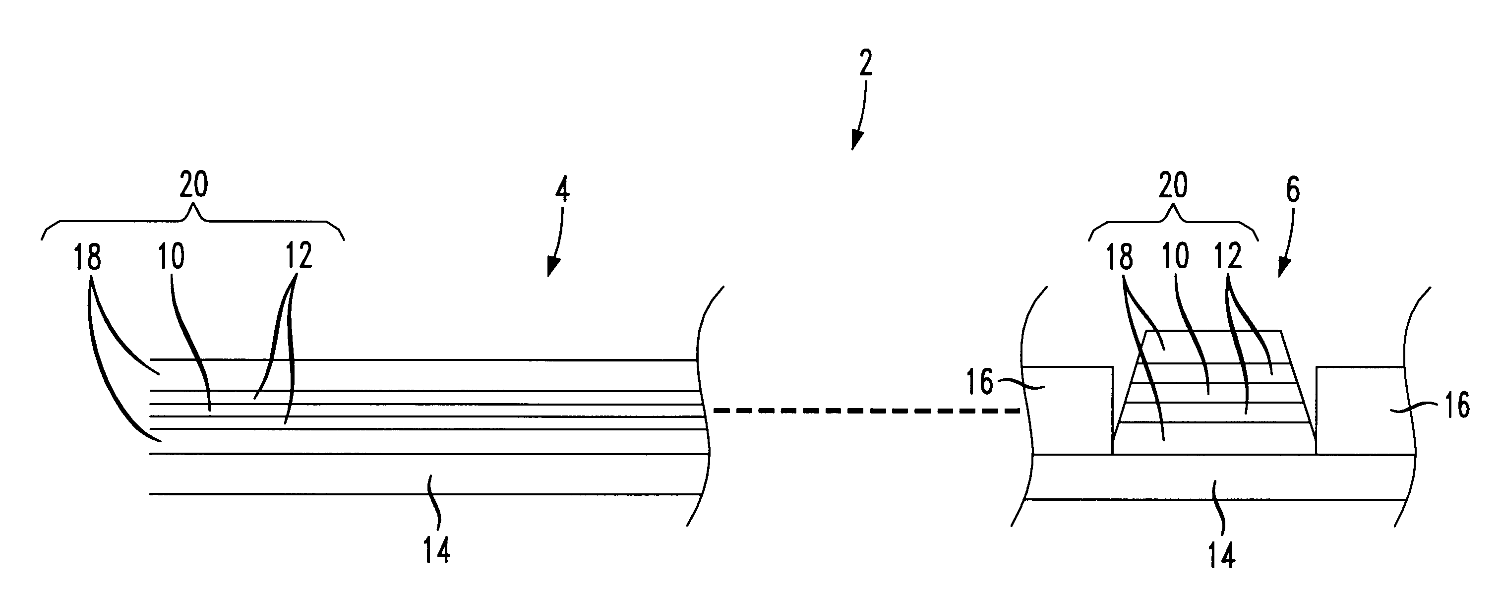
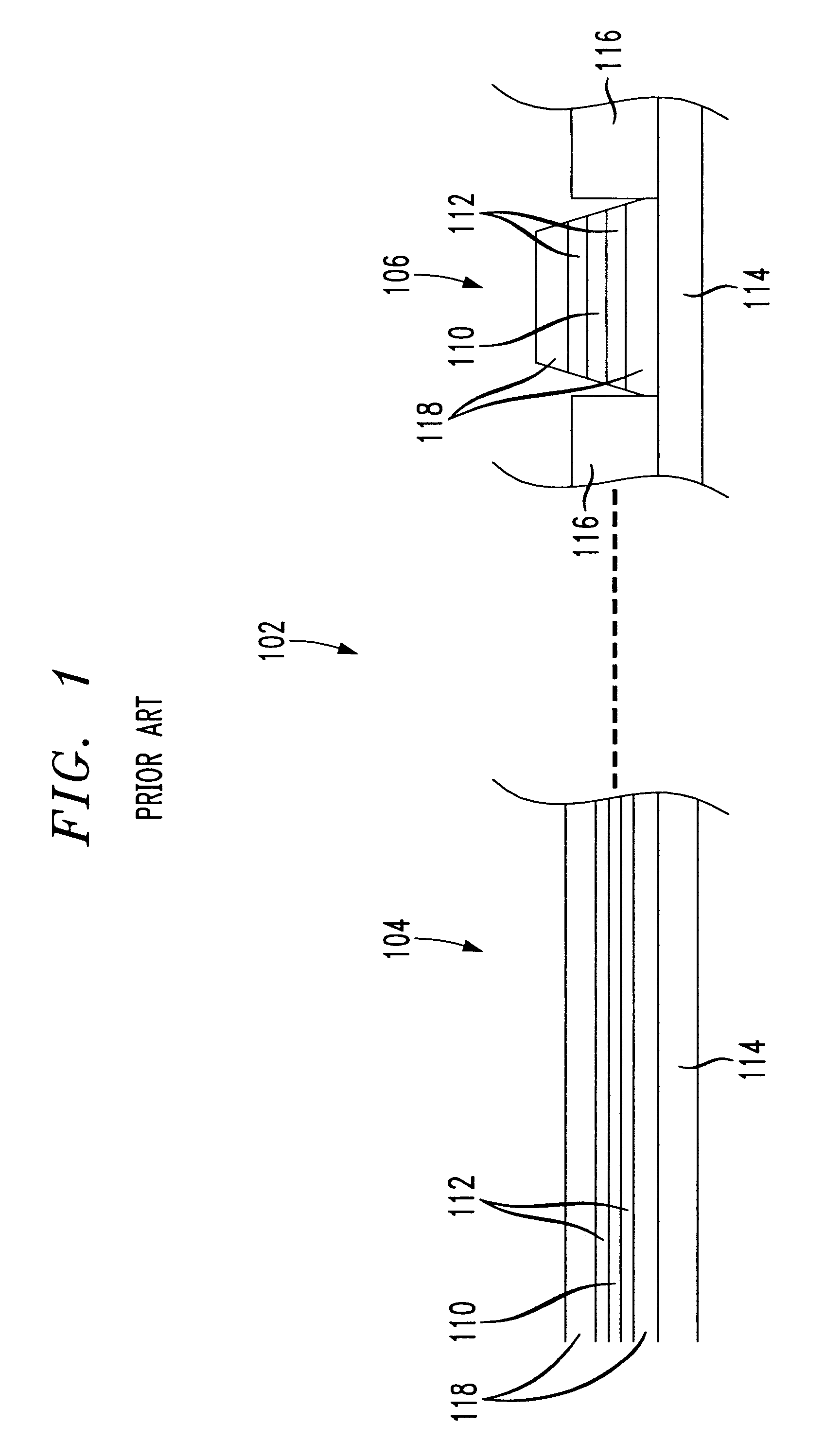
In accordance with the present invention, the net strain of a multiple quantum well (MQW) configuration of a semiconductor device is controlled by selecting different gallium precursor materials for the formation of the barrier and well layers of the MQW configuration.

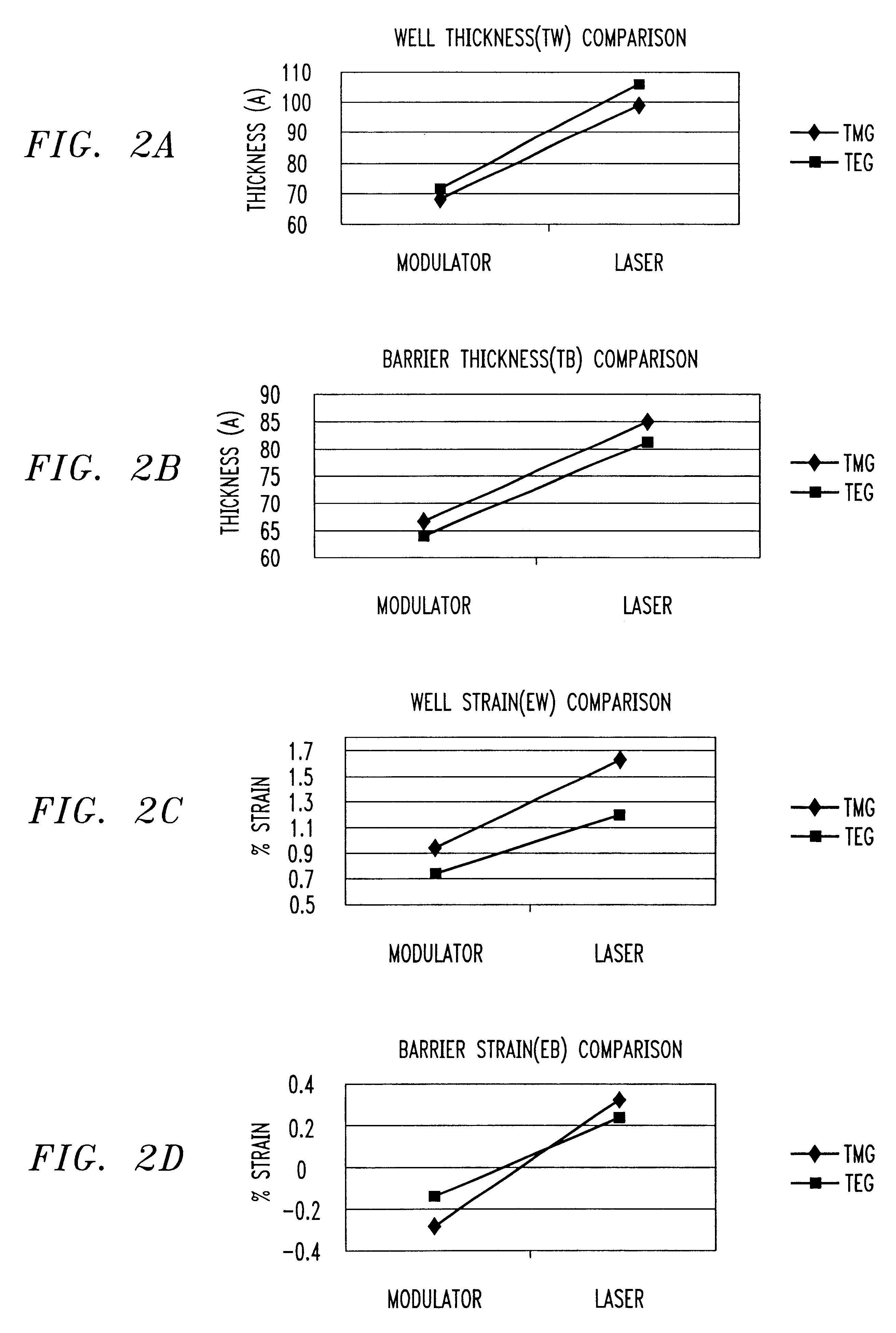
Quaternary composition layers of GaInAsP are used for forming the epitaxial layers of the MQW configuration. These compositions are formed by a metallo-organic chemical vapor deposition (MOCVD) in which precursor materials are introduced into a chamber with a gas for forming the layers on a substrate. In accordance with the invention, it has been found that changing a gallium precursor material from triethylgallium (TEG) to trimethylgallium (TMG) affects the strain and thickness of the layers being formed. Each of the graphs in FIGS. 2a-2d shows a comparison between the thickness or strain in the modulator region and the laser region for first and second types of epitaxial layer compositions of a multiple quantum well ...


PUM


Abstract

A semiconductor device including first and second epitaxial layers grown in a selective area growth region on a substrate includes an active layer or well layer comprising a first composition formed using a trimethylgallium precursor material and a barrier layer comprising a second composition formed using a triethylgallium precursor material. The use of the first and second compositions in the well layer and barrier layer respectively maximizes the strain in the well layer while simultaneously minimizing the net strain of the selective area growth region.

Description

1. Field of the InventionThe present invention relates to a semiconductor device having a heterostructure with a plurality of active material well layers alternately grown between a plurality of barrier layers and having a reduced net strain. More specifically, the present invention relates to an integrated semiconductor laser-modulator device exhibiting a reduced net strain, and to a process for manufacturing such a semiconductor device.2. Description of the Related ArtDuring the manufacturing of heterojunction semiconductor devices, each individual layer is grown epitaxially using one of many known growth techniques such, for example, as metal-organic chemical vapor deposition (MOCVD). Several layers are usually grown when producing a multiple quantum well (MQW) semiconductor such as an MQW laser so that alternating layers of active material well layers and barrier material layers are grown. In addition, the alternating layers are bound between a pair of separate confinement layer...

Claims


Application Information

Patent Timeline
Patent Type & Authority Patents(United States)
IPC IPC(8): H01S5/00H01S5/026H01S5/20
CPCH01S5/0265H01S5/2077
Inventor GLEW, RICHARD W.GRENKO, JUDITH A.
Owner LUCENT TECH INC
Why Eureka
Try Eureka