Emissive element and display device using such element

a technology of emissive elements and display devices, which is applied in the direction of static indicating devices, discharge tubes luminescent screens, instruments, etc., can solve the problems of accelerating the deterioration of the emissive layer, pixel deficiency display, and irregular surface creation

Inactive Publication Date: 2001-06-12
SANYO ELECTRIC CO LTD
View PDF9 Cites 434 Cited by
  • Summary
  • Abstract
  • Description
  • Claims
  • Application Information

AI Technical Summary

Problems solved by technology

The poor coverage may also result at irregularities in the surface created by the TFT through, for example, the thickness of the Al wiring.
In such cases, pixels produce deficient displays.
Another existing problem is that an electric field becomes concentrated at the uneven portions created by the thickness of the anode 81, especially at the edges on the peripheral portions of the anode 81, thereby speeding up the deterioration of the emissive layer.
A further disadvantage is that some of the emitted light irradiates the TFT underneath the emissive element layer.
Because of such light, leakage current of the TFT increases, and stable TFT characteristics and stable display cannot be achieved.
Furthermore, the insulating layer covering the peripheral portion of the first electrode reduces concentration of electric field at this peripheral portion, and thereby reduces characteristics deterioration of the overlying emissive element layer.
Light-shielding and / or light-absorbing properties of the insulating film can prevent external light or reflected light from the second electrode from entering other adjacent pixels which can result in display blurs and, in the case of a color display, deterioration of color purity caused by mixing of colors from other pixels.
That is, if light from the emissive element layer reaches the TFT, leakage current of the TFT is likely to increase.

Method used


Image

  • Emissive element and display device using such element
  • Emissive element and display device using such element
  • Emissive element and display device using such element

Examples


first embodiment

The present embodiment differs from the first embodiment in that only one TFT is provided for driving the EL element 60, and that the anode 61 is formed over the interlayer insulating film 15.

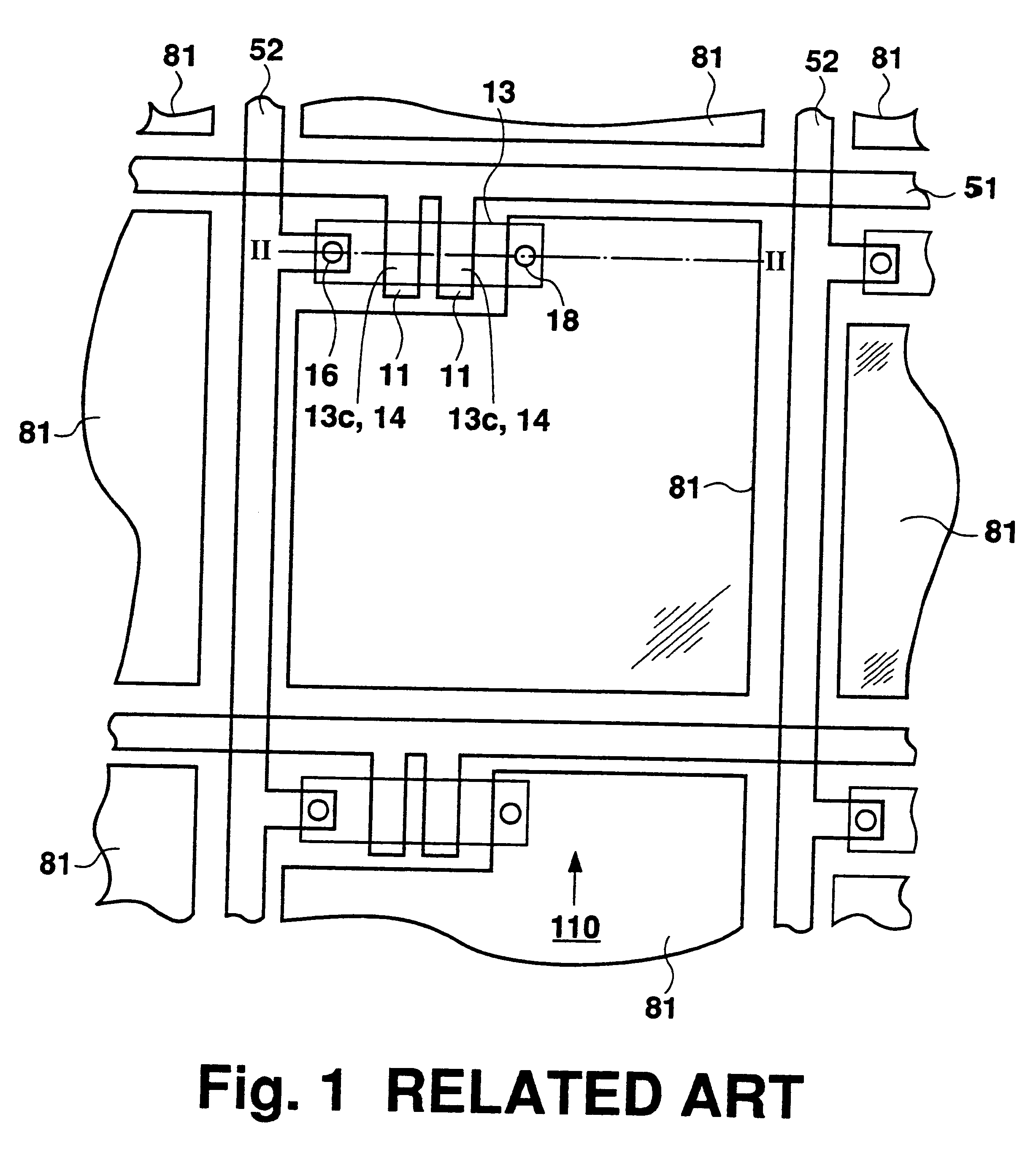
As shown in FIGS. 6 and 7, TFT 30 is disposed near a junction of a gate signal line 51 and a drain signal line 52. The source 13s of the TFT 30 is connected to the anode 61 of the organic EL element 60.

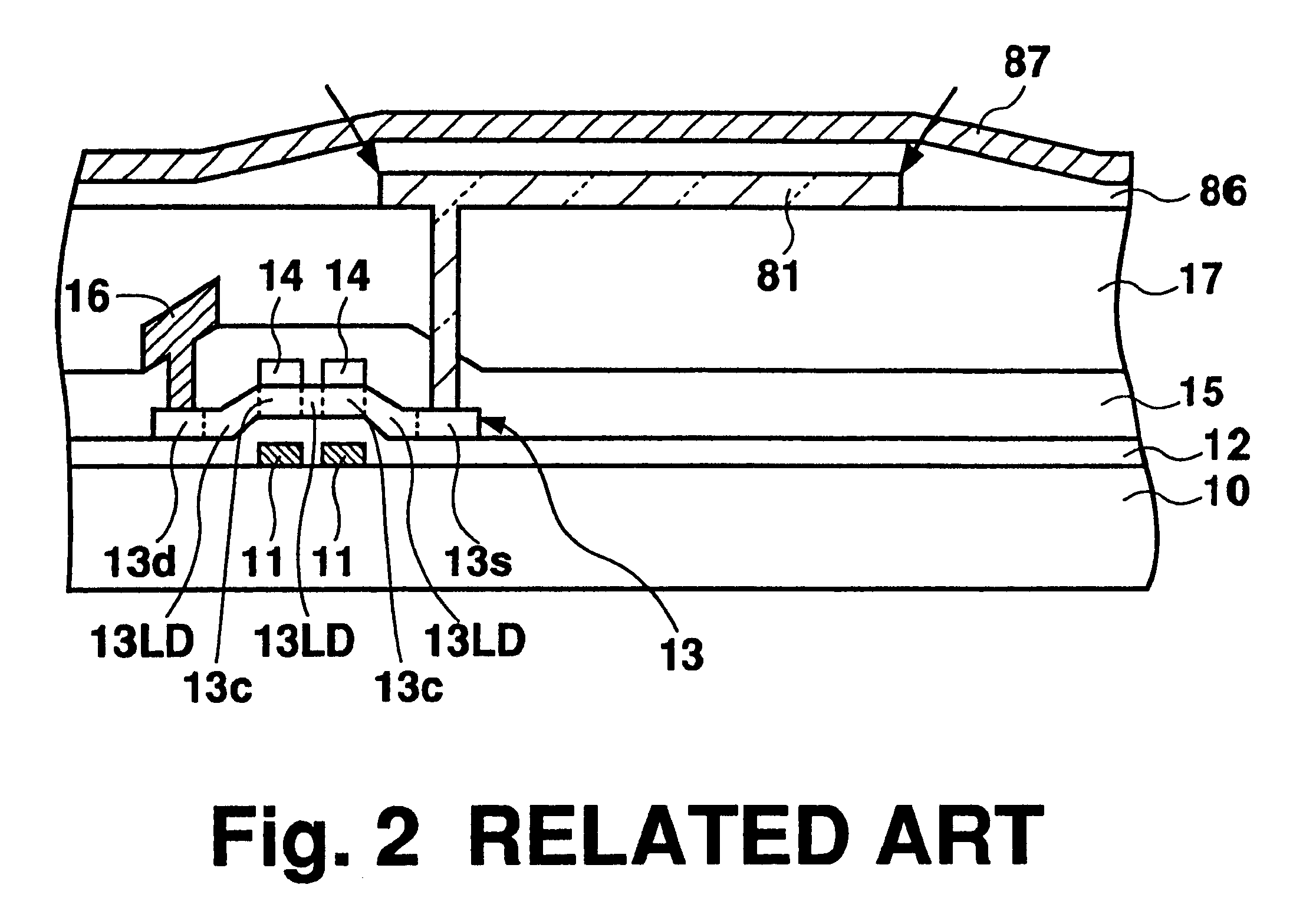
As shown in FIG. 7, the display pixel 110 is formed by sequentially laminating TFT and an organic EL element on a substrate 10 which may be an insulator substrate made of glass or synthetic resin, a conductive substrate, or a semiconductor substrate. When a conductive substrate or a semiconductor substrate is used as the substrate 10, an insulating film 32 made of materials such as SiO.sub.2 or SiN is deposited on the substrate 10 before forming the TFT.

As shown in FIG. 7, gate electrodes 11 composed of refractory metal such as Cr or Mo and a gate signal line 51 connected to the gate electrodes 1...

third embodiment

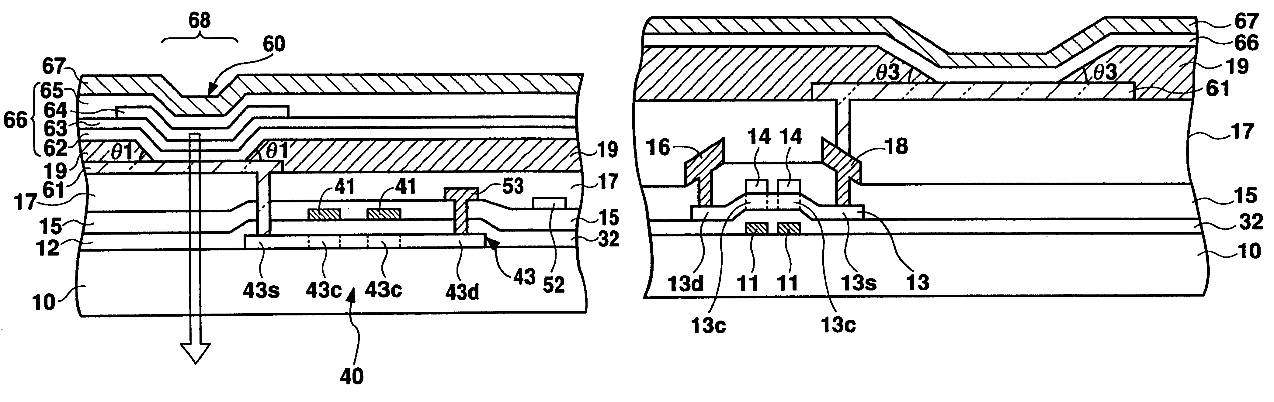
FIG. 8 is a cross-sectional view of an organic EL display device according to the present invention. The plan configuration of this embodiment is identical with the above-described FIG. 6, and FIG. 8 shows a cross-sectional view taken along line I--I in FIG. 6.

As shown in FIG. 8, the present embodiment differs from the second embodiment mainly in the structure between the source region 13s of TFT 30 and the anode 61 of the EL element. In the present embodiment, the contact holes formed in the interlayer insulating film 15 are filled with metal such as Al to provide the drain electrode 16 and the source electrode 18. The planarizing insulating film 17 is then deposited to planarize the surface. A contact hole is formed in the planarizing insulating film 17 at a location corresponding to the source electrode. Through this contact hole, the transparent electrode 61 is formed which is composed of a transparent conductive material such as ITO. Subsequently, the insulating film 19 is disp...


PUM


Abstract

An EL element (60) comprises an anode (61), a cathode (67), and an emissive element layer (66) interposed between the two electrodes. A TFT is connected to the anode (61) at its source electrode (33s). The peripheral portion of the anode (61) and the entire region over the TFT are covered with a planarizing insulating film (17), and a part of the exposed portion of the anode (61) is connected to the emissive element layer (66). According to the above arrangement, it is possible to prevent disconnection of the emissive element layer (66) which may be caused by an uneven surface created by the thickness of the anode (61), and to avoid formation of a short circuit between the anode (61) and the cathode (67).

Description

1. Field of the InventionThe present invention relates to a display device using a self-luminous element, and particularly to a display device using an electroluminescence element and a thin-film transistor.2. Description of the Related ArtIn recent years, electroluminescence (referred to hereinafter as "EL") display devices comprising EL elements are regarded as devices that may replace CRT and LCD. Research has been conducted for the development of EL display devices using, for example, thin film transistors (referred to hereinafter as "TFT") as switching elements to drive the EL elements.FIG. 1 shows a plan view of a possible configuration of an active type EL display device, and FIG. 2 shows a cross-sectional view taken along line II--II of FIG. 1.As shown in FIG. 1, a TFT is disposed near a junction of a gate signal line 51 with gate electrodes 11 and a drain signal line 52. The drain of the TFT is connected to the drain signal line 52, and the gate of the TFT is connected to t...

Claims


Application Information

Patent Timeline
Patent Type & Authority Patents(United States)
IPC IPC(8): H01L27/28H01L27/32H05B33/00
CPCH01L27/3246H01L51/5284H01L27/3272H10K59/122H10K59/126H10K50/865H05B33/00
Inventor YAMADA, TSUTOMU
Owner SANYO ELECTRIC CO LTD
Why Eureka
Try Eureka