Method to plate C4 to copper stud

a technology of copper studs and plate c4, which is applied in the direction of transportation and packaging, chemical coating, liquid/solution decomposition, etc., can solve the problems of insulator adjacent severe eroded, more problemsome insulator gap filling and planarization, and dishing on the larger features, etc., to achieve less expensive, eliminate the plating of metal on the pin, and improve productivity

Inactive Publication Date: 2001-06-26
ULTRATECH INT INC
View PDF19 Cites 64 Cited by
  • Summary
  • Abstract
  • Description
  • Claims
  • Application Information

AI Technical Summary

Benefits of technology

According to a particular application, an object of the present invention is to provide a process that permits attaching C4 solder balls directly to a final metal level in and / or on a substrate without requiring the utilization of a mask typical of traditional processes.
An advantage of the present invention is that it provides a less expensive process that known process for producing similar results.
Another advantage of the present invention is that it may utilize a barrier metal to carry plating current.
A further advantage of the present invention is that it may eliminate plating of metal on pins.
An additional advantage of the present invention is that is may provide higher productivity as compared to known processes.

Problems solved by technology

Also, insulator gap fill and planarization may be more problematic.
During metal chemical-mechanical polishing (CMP), the additional time needed to remove the excess metal overburden on the overplated smaller features causes dishing on the larger features.
Also, because of the prolonged polishing times, insulator adjacent may severely erode.
Severe dishing and insulator erosion in large metal features is a source of yield loss, especially when the occur at lower levels.
Here they cause trapped metal defects at the next higher level.
The longer time needed to remove the thicker metal overburden of the smallest metal lines and vias is one of the main culprits responsible for the low thruput and yield losses in the metal CMP process.
In the CMP process, these relatively large metal structures are sensitive to dishing because of the prolonged polishing times.

Method used


Image

  • Method to plate C4 to copper stud
  • Method to plate C4 to copper stud
  • Method to plate C4 to copper stud

Examples


Embodiment Construction

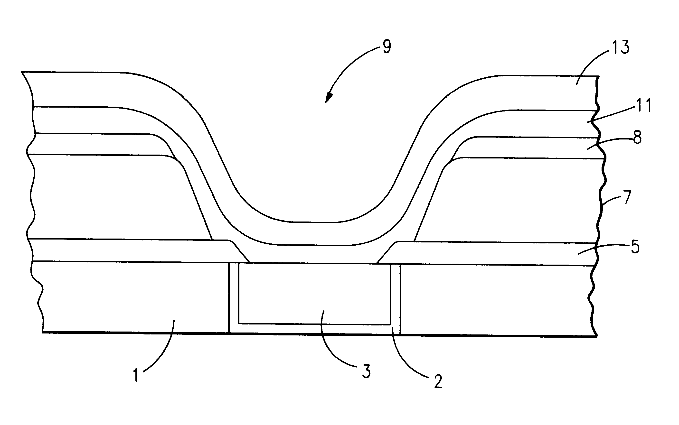
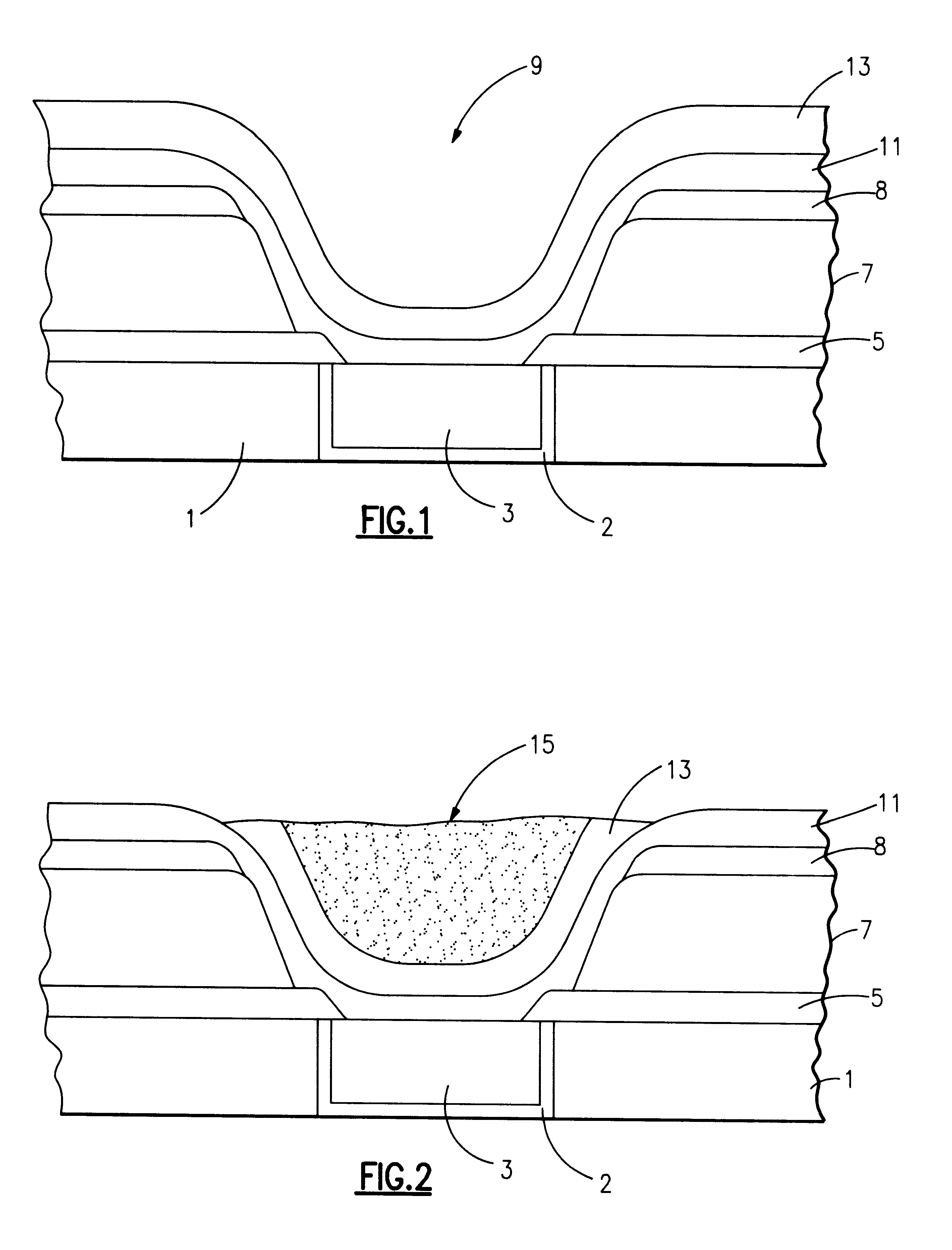
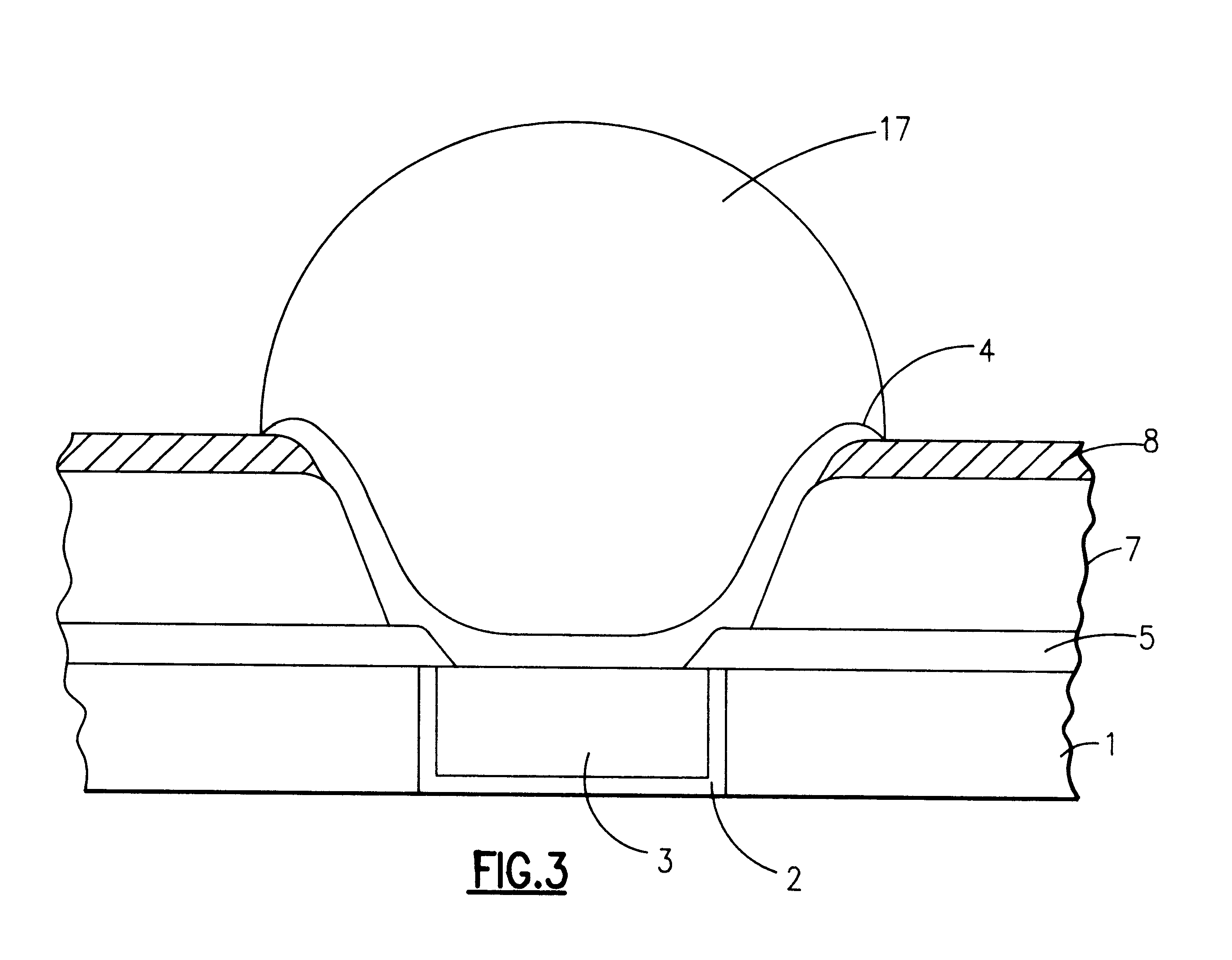
As described above, the present invention relates to electroplating a second metal on a metal feature of a first metal wherein the metal feature is arranged in and / or on a substrate. The present invention permits the second metal to be electroplated without utilizing a mask.

To carry out this process, methods of the present invention utilize a highly conducting barrier film alpha-Ta to carry current and selectively plate recesses in semiconducting and non-semiconducting substrates. The methods according to the present invention include providing a substrate. Various features may be provide in the substrate for accomplishing various tasks.

For example, the various features made of conductive material may be provided in and / or on the substrate. One example of such a feature is a metal last formed in the substrate. According to one example, the last is made of copper. However, as stated above, other features may be provided in the substrate having other forms and functions and made of ot...


PUM

PropertyMeasurementUnit
thickaaaaaaaaaa
thickaaaaaaaaaa
thickaaaaaaaaaa

Abstract

A method for plating a second metal directly to a first metal without utilizing a mask. A semiconductor substrate is provided including at least one metal feature and at least one insulating layer covering the metal feature and the substrate. At least one recess is formed in the at least one insulating layer thereby exposing at least a portion of the metal feature. At least one conductive barrier layer is formed over the insulating layer and the exposed portion of the metal feature. A plating seed layer of a first metal is formed over the at least one barrier layer. A photoresist layer is deposited over the plating seed layer. Portions of the photoresist layer and of the plating seed layer outside of the at least one recess are removed. Photoresist remaining in the at least one recess is removed. A second metal is electroplated to the plating seed layer in the recess.

Description

The present invention relates to a process for plating a conductive material to a conductive feature in and / or on a substrate. More particularly, the present invention concerns electroplating a conductive material to a metal feature in and / or on a substrate using a highly conducting barrier film to conduct electrical current. In particular, the present invention provides methods for electroplating a solder ball utilized in a controlled collapse chip connection (C4) process to a metal feature provided in and / or on a substrate. Additionally, the present invention provides semiconductor structures prepared according to processes of the present invention.Various techniques have been investigated and utilized for attaching conductive material to semiconductor chips. These methods include the lift-off process, thru-mask methods, metal reactive ion etch (RIE) and metal and insulator damascene and various combinations of the above-listed methods. The lift-off and thru-mask methods are more ...

Claims


Application Information

Patent Timeline
Patent Type & Authority Patents(United States)
IPC IPC(8): H01L21/02H01L21/60C25D7/12C23C18/31H01L21/288
CPCH01L24/03H01L24/05H01L24/11H01L2924/0002Y10T428/12361Y10T428/12299H01L2224/0401H01L2924/0001H01L2224/13111H01L24/13H01L2224/0345H01L2224/03602H01L2224/03912H01L2224/04042H01L2224/05572H01L2224/1148H01L2224/13006H01L2224/13022H01L2224/13099H01L2924/01004H01L2924/01013H01L2924/01029H01L2924/01073H01L2924/01074H01L2924/01078H01L2924/01079H01L2924/01082H01L2924/01322H01L2924/014H01L2924/04953H01L2924/3025H01L2924/01006H01L2924/01023H01L2924/01033H01L2924/0105H01L2924/00014H01L2224/05552
Inventor UZOH, CYPRIAN EMEKAEDELSTEIN, DANIEL C.
Owner ULTRATECH INT INC
Why Eureka
Try Eureka