Micro-machining

a micro-machining and micro-machining technology, applied in the direction of acceleration measurement using interia force, turn-sensitive devices, instruments, etc., can solve the problems of layer delamination, difficult control of material uniformity, and inability to reliably deposit materials, etc., to offset the higher cost of wafers

Inactive Publication Date: 2001-08-21
QINETIQ LTD
View PDF20 Cites 57 Cited by
  • Summary
  • Abstract
  • Description
  • Claims
  • Application Information

AI Technical Summary

Benefits of technology

may more than offset the higher cost of the wafer

Problems solved by technology

It would not have been possible to reliably deposit material to the depth achieved by the present method.
For instance providing material by deposition has the problem that the uniformity of the material is hard to control with errors of 5% across a wafer being typical.
Further, as the thickness of a deposited layer increases the internal stresses within the layer of deposited material increase and can eventually lead to the deposited layer delaminating itself from the material upon which the material was deposited.
However, the single crystal of the wafer often shows anisotropic properties and considerations may arise which need to be considered in the design stage to account for the anisotropic nature.
Such a structure is equally possible but the interface between the mechanical wafer and the insulating layer tends to be of poorer quality since this is where bonding occurs.
In some prior art methods a wafer which was not supported over its entire area was polished which in some instances led to buckling of the wafer over the unsupported areas.
When using wet etchants stiction problems may arise due to surface tension effects as the etchant dries causing the suspended portions to stick to the other wafer or to portions of the etched wafer above the predetermined cross sectional area.
Stiction problems associated with having wet surfaces between the suspended portions and the remainder of the first and second wafers are therefo

Method used


Image

  • Micro-machining
  • Micro-machining
  • Micro-machining

Examples


Embodiment Construction

with reference to the accompanying drawings of which:

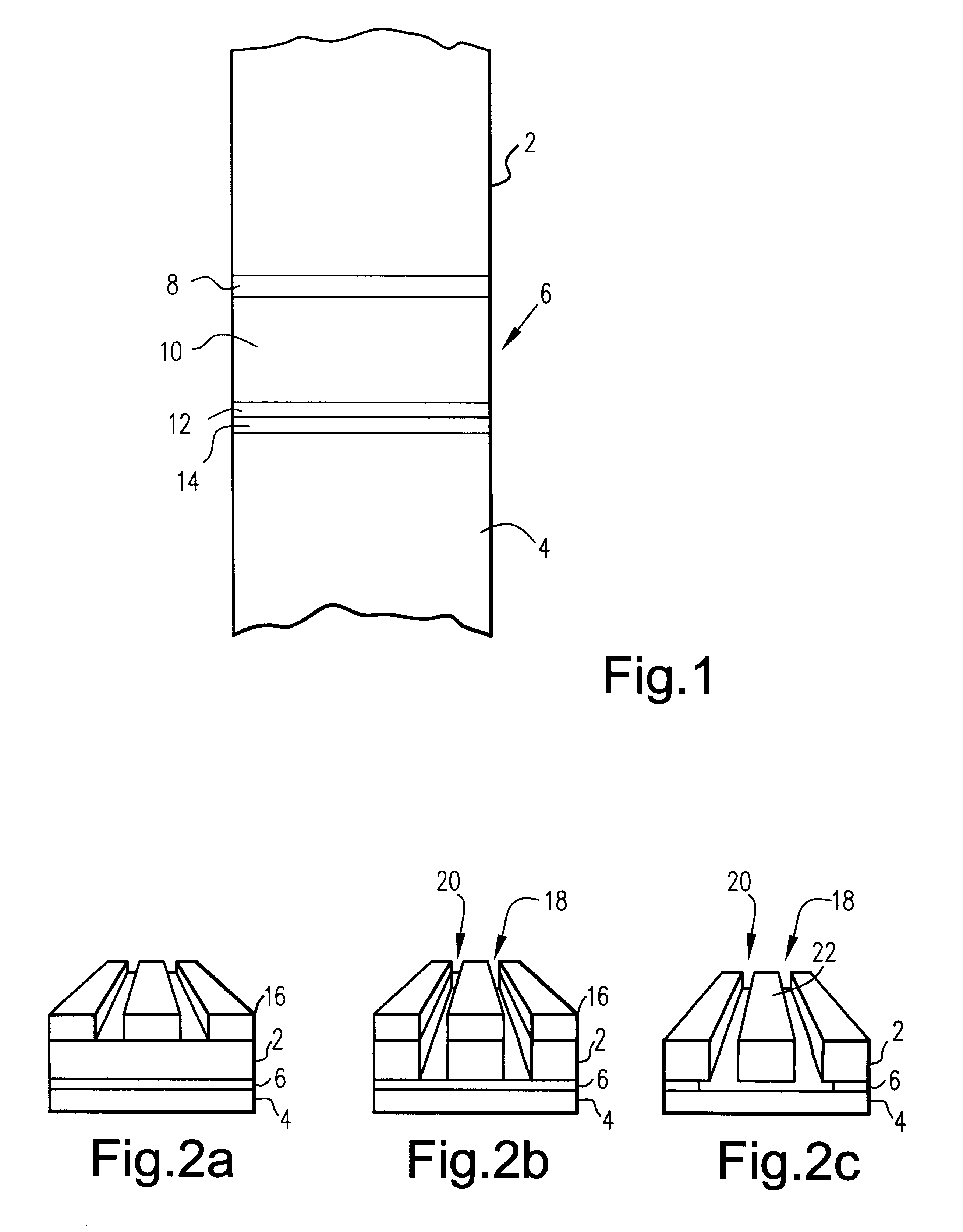
FIG. 1 shows a cross section through two silicon wafers separated by a plurality of insulating layers;

FIGS. 2a to c shows stages in the production of a micro-mechanical sensor according to the invention;

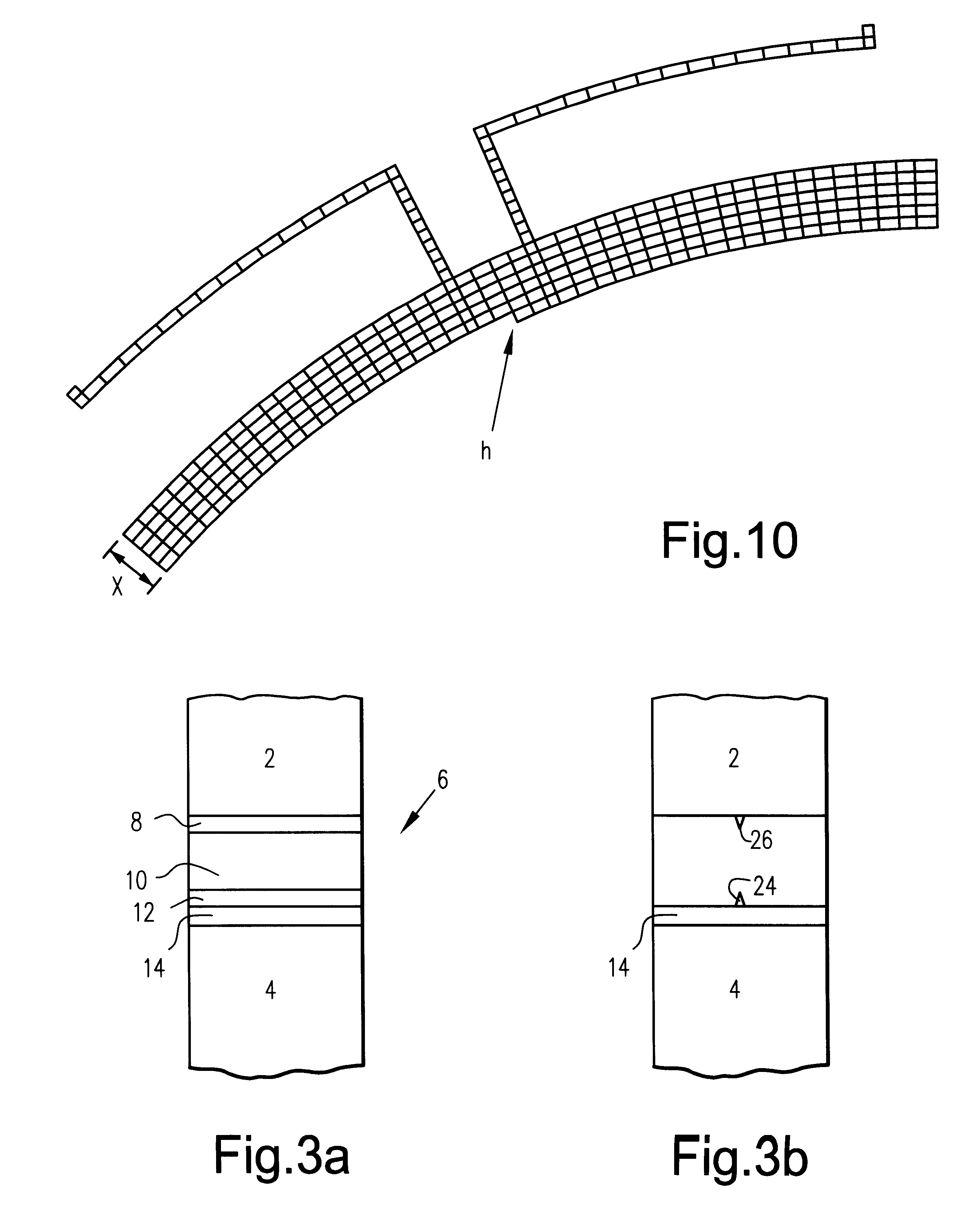
FIGS. 3a-b shows the principle involved in reducing the stiction between two wafers;

FIGS. 4a-b shows the stages in a different process to that shown in FIG. 2 of the production of a micro-mechanical sensor;

FIGS. 5a-e shows a schematic for a further process flow for the production of a micro-mechanical sensor;

FIG. 6 shows a scanning electron microscope picture of a micro-mechanical sensor formed according to the present invention;

FIG. 7 shows a scanning electron microscope picture of a feature of the sensor of FIG. 6;

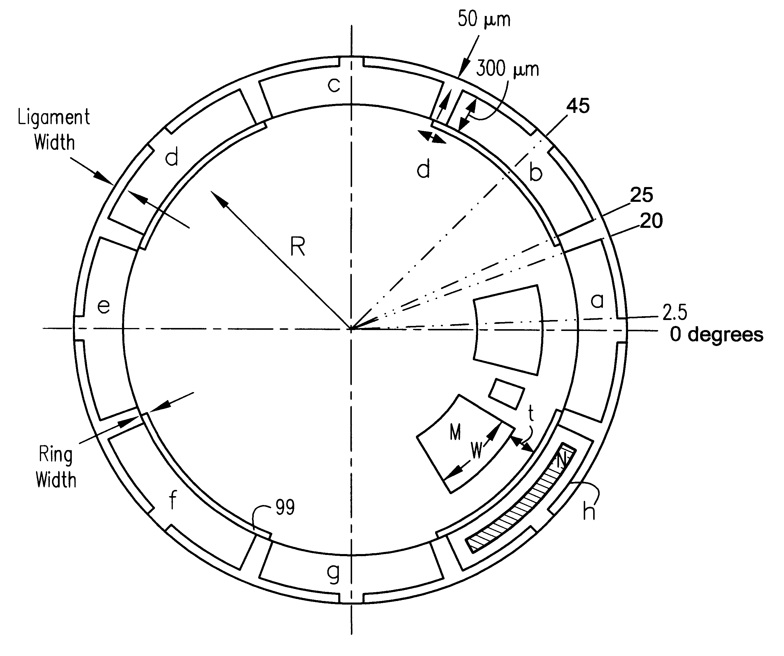
FIG. 8 shows a schematic structure of a gyroscope according to the present invention;

FIGS. 9a and 9b show the primary and secondary modes of vibration of the gyroscope of FIG. 8 respectively; and

FIG. 10 shows a portion ...


PUM


Abstract

A method of fabricating a micro-mechanical sensor (101) comprising the steps for forming an insulating layer (6) onto the surface of a first wafer (4) bonding a second wafer (2) to the insulating layer (6), patterning and subsequently etching either the first (4) or second wafer (6) such that channels (18, 20) are created in either the first (2) or second (4) wafer terminating adjacent the insulating layer (6) and etching the insulating layer (6) to remove portions of the insulating layer (6) below the etched wafer such that those portions of the etched wafer below a predetermined cross section, suspended portions (22), become substantially freely suspended above the un-etched wafer. This method uses Silicon on Insulator technology. Also disclosed is a micro-mechanical gyroscope structure (101) allowing an anisotropic silicon to be used to fabricate a sensor functioning as if fabricated from isotropic silicon.

Description

1. Field of the InventionThis invention relates to improvements in micro-machining, perhaps in a particular example to improvements in manufacturing motion sensors.2. Discussion of Prior ArtIt is known to produce micro-mechanical sensors using micro-machining techniques. In particular, GB 2,276,976 shows a particular method for the production of such a sensor wherein a silicon wafer has cavities formed into its surface. Next a second wafer is bonded to the surface of the first wafer and the second wafer etched in a manner to release portions of the second wafer which are above the cavities in the first wafer. Thus, suspended resonating portions are formed which exist above the cavities in the first wafer.Further, WO 95 / 08775 shows a structure wherein a layer of silicon is formed onto a substrate. The silicon is etched in a manner to form suspended resonator portions above cavities in the silicon.One such micro-mechanical sensor is the vibratory gyroscope which measures the rate of t...

Claims


Application Information

Patent Timeline
IPC IPC(8): G01C19/56H01L29/84
CPCG01C19/56H01L29/84
Inventor MCNIE, MARK E.NAYAR, VISHAL
Owner QINETIQ LTD
Why Eureka
Try Eureka