Method for synthesizing single crystal AIN thin films of low resistivity n-type and low resistivity p-type

a single crystal ain thin film, low resistivity technology, applied in the direction of crystal growth process, polycrystalline material growth, chemistry apparatus and processes, etc., can solve the problem that the carrier cannot be activated at room temperatur

Inactive Publication Date: 2001-08-28
JAPAN SCI & TECH CORP
View PDF4 Cites 8 Cited by
  • Summary
  • Abstract
  • Description
  • Claims
  • Application Information

AI Technical Summary

Problems solved by technology

However, since an AlN has a large band gap energy such as 6.5 eV, and an acceptor or a donor itse

Method used


Image

  • Method for synthesizing single crystal AIN thin films of low resistivity n-type and low resistivity p-type
  • Method for synthesizing single crystal AIN thin films of low resistivity n-type and low resistivity p-type
  • Method for synthesizing single crystal AIN thin films of low resistivity n-type and low resistivity p-type

Examples


examples

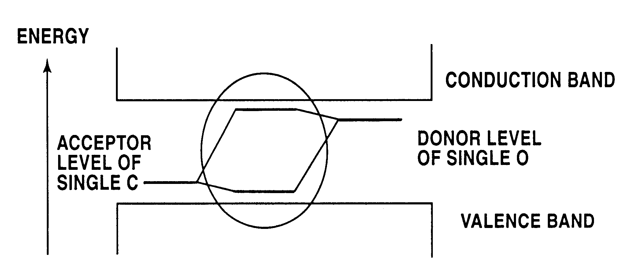
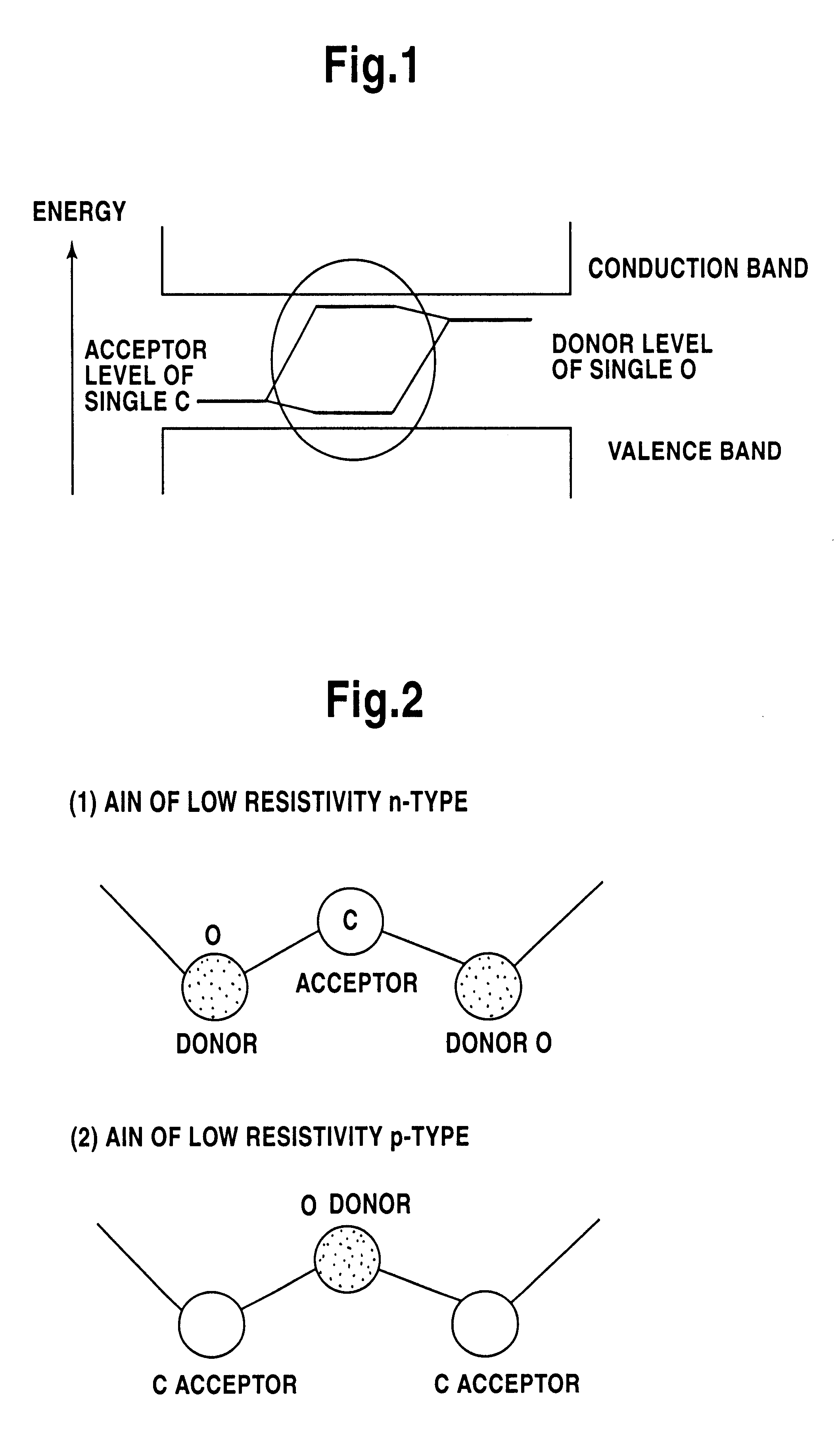
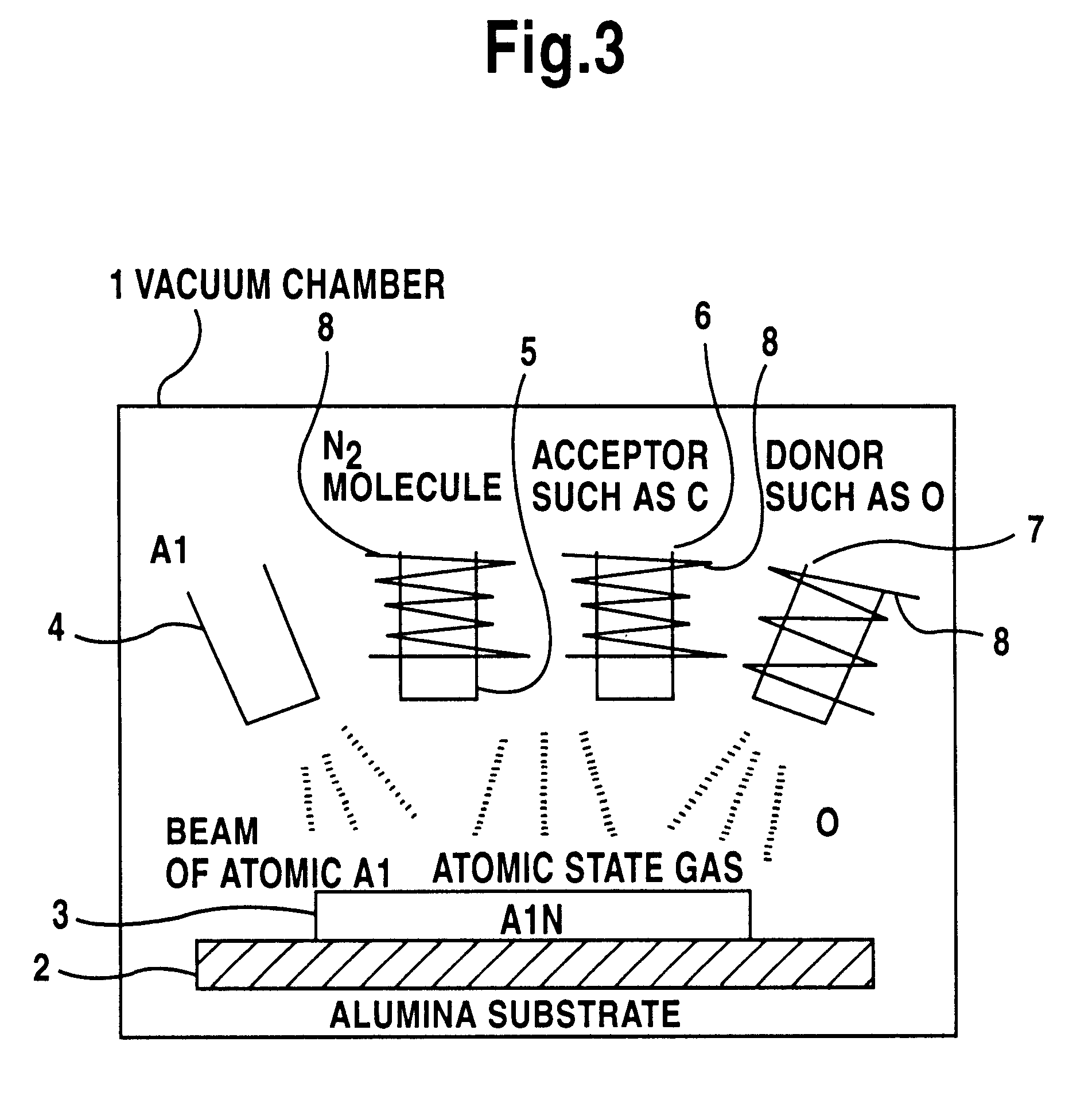
As shown in FIG. 3, the vacuum chamber 1 was maintained to be vacuum degree of 10.sup.-10 torr, and the alumina substrate 2 was heated by the electrical heater. The Al was heated by an oven heater to irradiate a beam of an atomic Al toward the substrate 2. N.sub.2 molecule was excited by the RF coil 8 to supply atomic gas flows of N+ or N.sub.2 in an excited state toward the substrate 2 so as to be adhered to the substrate 2. C as an acceptor was emitted toward the substrate 2 from the introducing pipe 6 at the flow rate of 10.sup.-9 torr and O as a donor was emitted toward the substrate 2 from the introducing pipe 7 at the flow rate of 5 .times.10.sup.-9 torr so as to simultaneously dope them to thereby form an AlN crystal at the substrate temperature of 600.degree. C., 650.degree. C., 800.degree. C., 1000.degree.C. and 1100.degree. C. The C as an acceptor and the O as a donor were electrically excited by the RF coil 8 so as to become an atomic gaseous state. After 120 minutes have...


PUM


Abstract

In growing single AlN thin films on a semiconductor substrate by rapidly cooling a beam of atomic Al and atomic or molecular N obtained by exciting or decomposing N2 with an electromagnetic wave on the semiconductor substrate, an n-type dopant and a p-type dopant in the form of atomic beams are simultaneously doped in a crystal, so that pairs of an n-type dopant and a p-type dopant are formed in the crystal to synthesize single crystal AlN thin films of low resistivity n-type and low resistivity p-type.

Description

This invention relates to a method for manufacturing single crystal AlN (aluminum nitride) thin films of low resistivity n-type and low resistivity p-type, which are expected to be used as next generation semiconductors.TECHNICAL BACKGROUNDA method for forming single crystal AlN thin films by a molecular beam epitaxy method, or the like, is known (for example, Japanese Patent Unexamined Publication Nos. H8(1996)-2999 and H9(1997)-309795).However, since an AlN has a large band gap energy such as 6.5 eV, and an acceptor or a donor itself has a low impurity level of 500 meV (4000K), carriers cannot be activated at room temperature. As a result, only AlN thin films of high resistivity can be obtained.OBJECTS TO BE SOLVED BY THE INVENTIONIf single crystal thin AlN films of low resistivity p-type and low-resistivity n-type can be synthesized, it is possible to manufacture a high power and high speed semiconductor device operable at high temperature and an ultraviolet semiconductor laser d...

Claims


Application Information

Patent Timeline
IPC IPC(8): C30B23/02H01L21/205H01L21/02H01L21/203C30B31/20C30B29/38H01L21/263
CPCC30B23/02C30B29/403H01L21/0242H01L21/02631H01L21/02576H01L21/02579H01L21/0262H01L21/0254
Inventor YOSHIDA, HIROSHI
Owner JAPAN SCI & TECH CORP
Why Eureka
Try Eureka