Method and apparatus for a semiconductor package for vertical surface mounting

a technology of semiconductor dice and package, applied in the direction of electrical apparatus casing/cabinet/drawer, printed circuit non-printed electric components association, instruments, etc., can solve the problems of difficult to make a reliable electrical connection to a bare die, thin and fragile bare dice, and large packaging space on the printed circuit board

Inactive Publication Date: 2001-09-18
MICRON TECH INC
View PDF13 Cites 291 Cited by
  • Summary
  • Abstract
  • Description
  • Claims
  • Application Information

AI Technical Summary

Problems solved by technology

One problem associated with conventionally packaged die is that the package occupies a relatively large amount of space on the printed circuit board.
However, because bare dice are thin and fragile, packages called connectors have been developed to electrically connect and house multiple bare dice for mounting a supporting substrate to a printed circuit board.
One problem with this type of connector is that it is difficult to make a reliable electrical connection to a bare die.
In addition, the bare die is often damaged during insertion into the connector.
Although encapsulation provides additional protection to the die, this method nevertheless suffers from some of the same deficiencies of previous methods.

Method used


Image

  • Method and apparatus for a semiconductor package for vertical surface mounting
  • Method and apparatus for a semiconductor package for vertical surface mounting
  • Method and apparatus for a semiconductor package for vertical surface mounting

Examples


Embodiment Construction

Illustrative embodiments of the invention are described below. In the interest of clarity, not all features of an actual implementation are described in this specification. It will of course be appreciated that in the development of any such actual embodiment, numerous implementation-specific decisions must be made to achieve the developers' specific goals, such as compliance with system-related and business-related constraints, which will vary from one implementation to another. Moreover, it will be appreciated that such a development effort might be complex and time-consuming, but would nevertheless be a routine undertaking for those of ordinary skill in the art having the benefit of this disclosure.

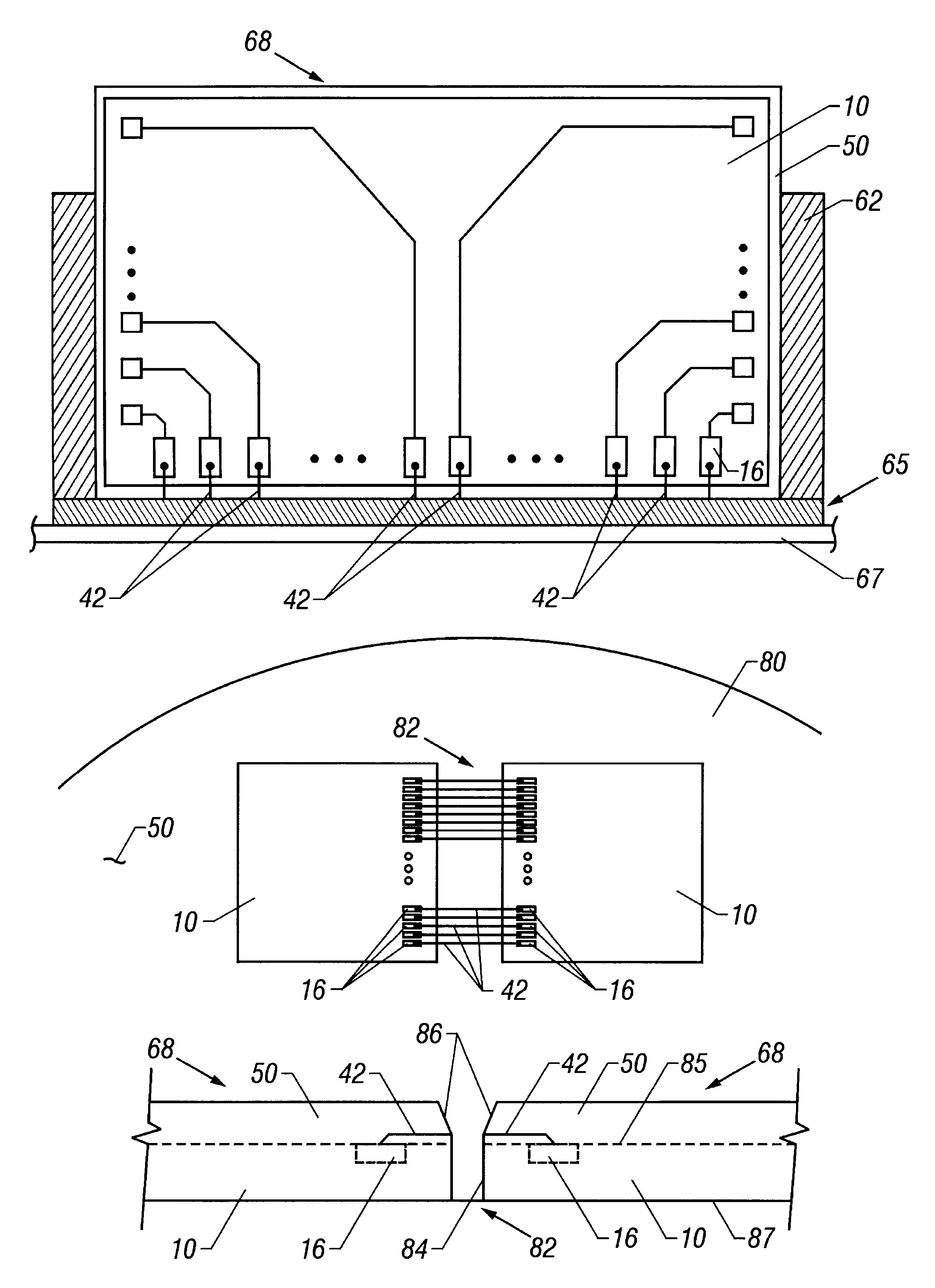
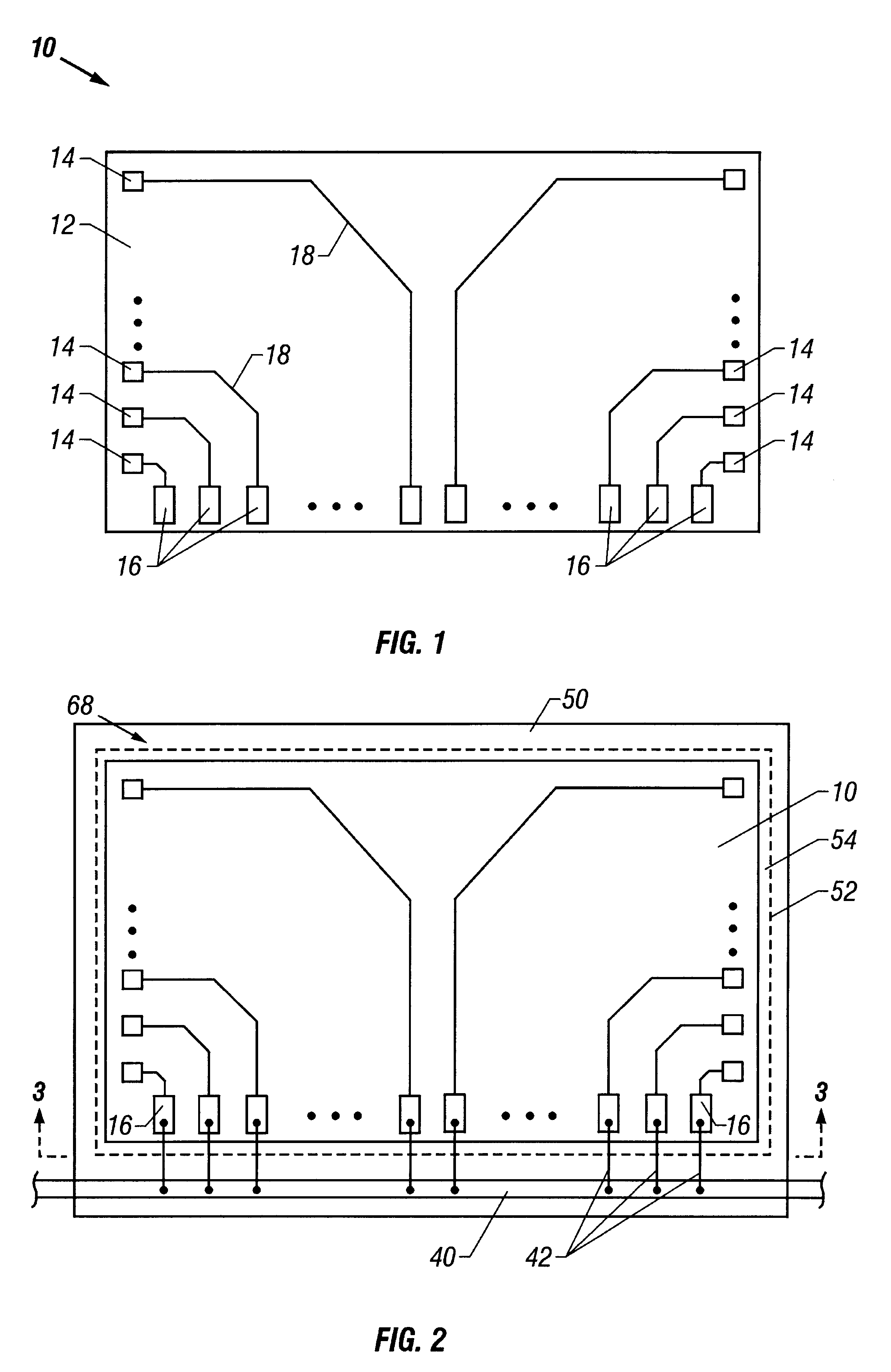
FIG. 1 is a plan view of an integrated circuit device 10 comprising a substrate 12 in which various electrical devices have been formed using techniques that are well known in the art. Formed on the substrate 12 is electrical circuitry (not shown) to interconnect the electrical devices...


PUM


Abstract

A method for packaging a semiconductor device includes connecting a plurality of wire leads to a corresponding plurality of electrical connection pads on the semiconductor device, covering at least a portion of the semiconductor device and at least a portion of each of the wire leads with an encapsulating material, and removing a portion of the encapsulating material and a portion of each of the wire leads to form a packaged semiconductor device wherein each of the wire leads has an exposed portion only at an end. The invention also includes a packaged semiconductor device having an integrated circuit device with a plurality of electrical connection pads, a plurality of wire leads coupled to the plurality of electrical connection pads, and a covering of encapsulating material covering at least a portion of the integrated circuit device and covering each of the wire leads, wherein each of the wire leads has an exposed end. The present invention contemplates wire bonding and encapsulation of individual die as well as multiple die on a single wafer.

Description

1. Field of the InventionThis invention relates generally to the packaging of semiconductor dice and, more particularly, to the packaging of semiconductor dice to facilitate vertical mounting on a printed circuit board.2. Description of the Related ArtSemiconductor dice are normally formed in large quantities on a wafer of semiconductor material, for example, silicon. After the dice are singulated from the wafer, they may be individually packaged in a plastic or ceramic package, for example. A lead frame may support the die for wire bonding and packaging and provide the lead system for the completed package. In general, electrical circuitry formed on the die is coupled to bond pads on the die to facilitate interconnection of the electrical circuitry with the outside world. During the wire bonding and packaging process, each bond pad is electrically connected by way of wire leads to the lead frame. The electrical connection includes a wire bond formed on the bond pad, a wire lead and...

Claims


Application Information

Patent Timeline
Patent Type & Authority Patents(United States)
IPC IPC(8): H01L23/52H01L23/31H01L23/28H01L23/528H01L25/065
CPCH01L23/3171H01L23/528H01L25/0657H01L24/49H01L24/48H01L2924/30107H01L2924/14H01L2225/06593H01L2224/48137H01L2224/48145H01L2224/49175H01L2225/06506H01L2225/0651H01L2225/06527H01L2225/06551H01L2225/06575H01L2225/06582H01L2924/00H01L2224/05599H01L2224/85399H01L2924/00014H01L2224/45099H01L2224/45015H01L2924/207H01L2924/00012
Inventor FARNWORTH, WARRENKINSMAN, LARRYMODEN, WALTER
Owner MICRON TECH INC
Why Eureka
Try Eureka