Process for self-alignment of sub-critical contacts to wiring

a technology of sub-critical contacts and wiring, which is applied in the direction of instruments, photomechanical devices, optics, etc., can solve the problems of difficult lithographic scaling of contact holes in integrated circuits, and the enhancement of isolated bright images by techniques such as contact holes is not easy to achiev

Inactive Publication Date: 2001-10-16
IBM CORP
View PDF5 Cites 50 Cited by
  • Summary
  • Abstract
  • Description
  • Claims
  • Application Information

AI Technical Summary

Problems solved by technology

It is known that the lithographic scaling of contact holes in integrated circuits is more difficult than the lithographic sealing of line/space patterns because the optical enhancement techniques of of...

Method used


Image

  • Process for self-alignment of sub-critical contacts to wiring
  • Process for self-alignment of sub-critical contacts to wiring
  • Process for self-alignment of sub-critical contacts to wiring

Examples


Embodiment Construction

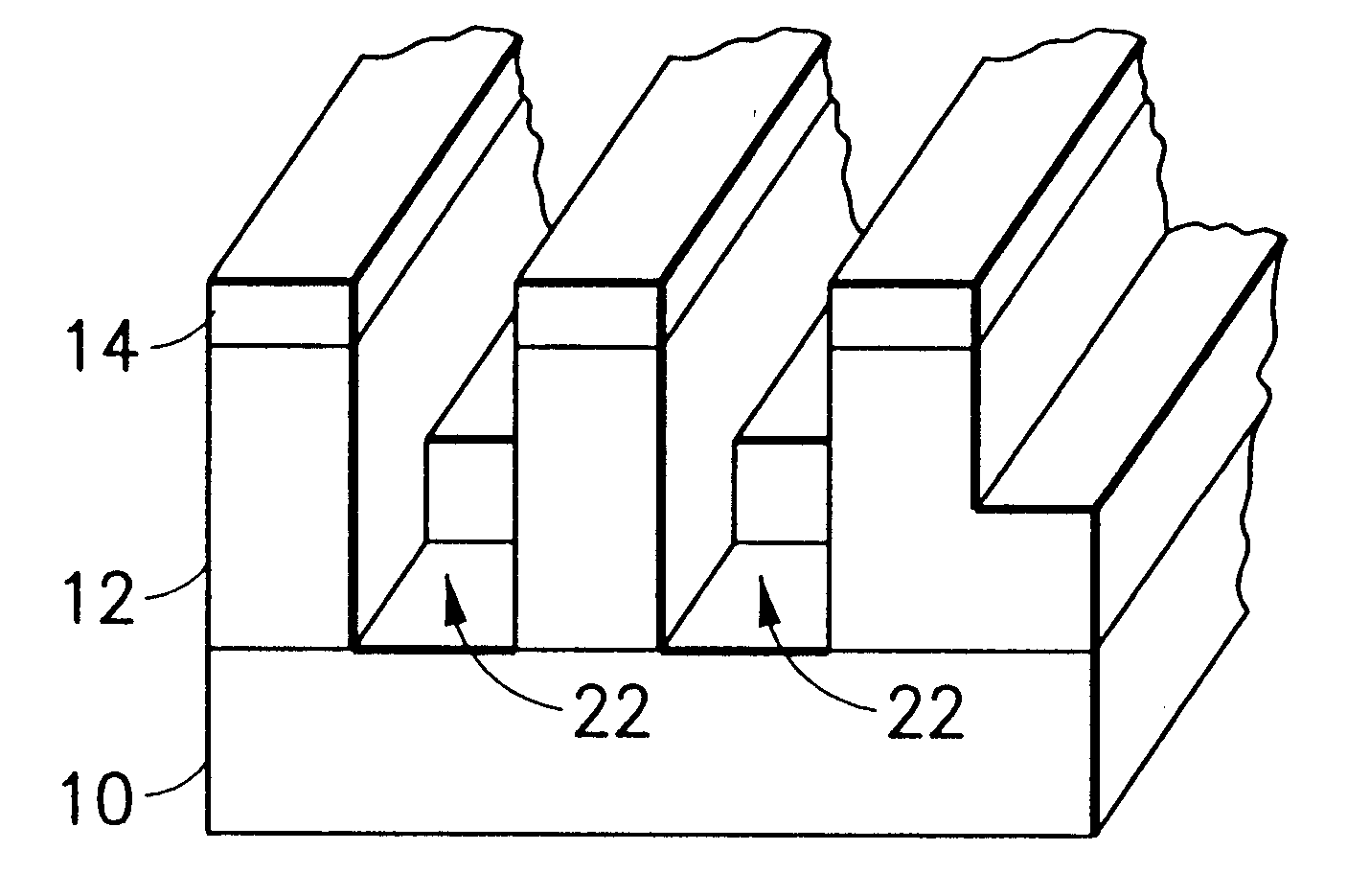
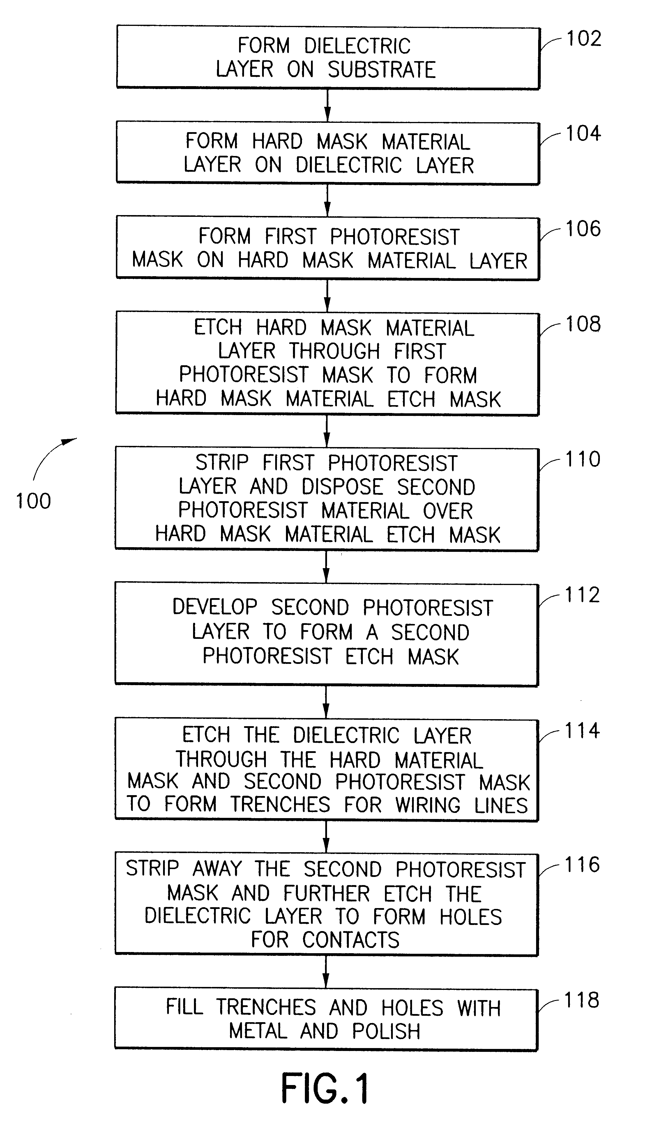
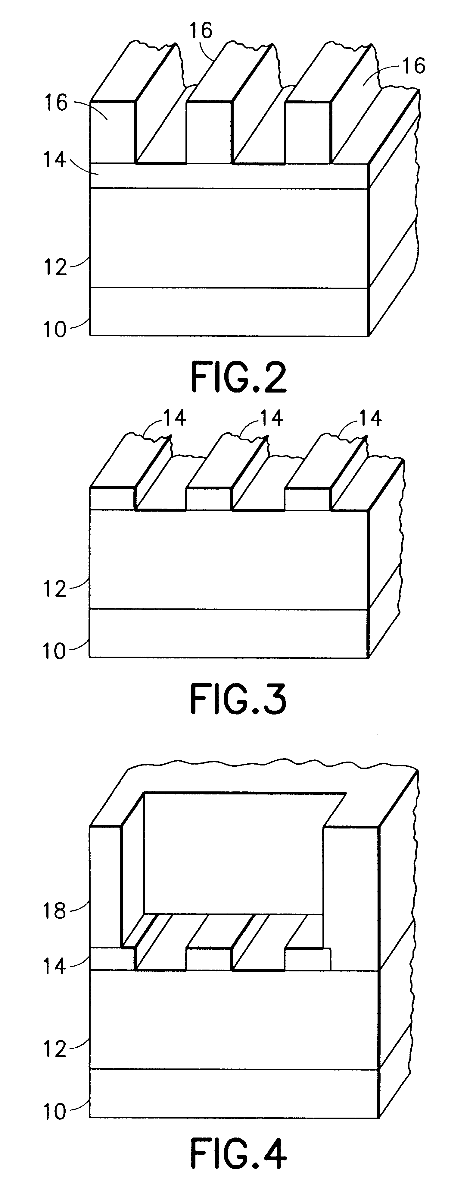
The present invention provides a method that forms contacts on an integrated circuit that are self-aligned with the wiring patterns of the integrated circuit. In the method the metal wiring is patterned first over an insulating substrate layer. The insulator layer is composed of two layers, one being a thicker layer underneath a thinner layer at the substrate surface. The wiring pattern trenches are etched through the thinner surface layer, and if desired, partially through the lower, thicker layer.

After the wiring pattern is etched, the contacts for the wiring layer are printed as line / space patterns which intersect the wiring pattern. The contact pattern is etched into the lower, thicker layer with an etch process that is selective to the thinner layer. As a result, the only location where a contact is formed is at the intersection of the wiring pattern with the photoresist space of the contact layer. The width of the contact is determined by the width of the wiring image and the ...


PUM


Abstract

A method for forming contacts on an integrated circuit that are self-aligned with the wiring patterns of the integrated circuit. In the method a thicker lower layer of a first material and a thinner upper layer of a second material are formed on a substrate. The features of the metal wiring is patterned first on the upper layer. The wiring pattern trenches are etched through the thinner surface layer, and partially through the second, thicker layer. After the wiring pattern is etched, the contacts for the wiring layer are printed as line/space patterns which intersect the wiring pattern. The contact pattern is etched into the lower, thicker layer with an etch process that is selective to the upper thinner layer. The contact is only formed at the intersection point of the wiring image with the contact image, therefore the contact is self-aligned to the metal.

Description

1. Technical FieldThe present invention relates to the fabrication of semiconductor microchip structures, and more particularly to methods for forming contact holes in microchips for establishing electrical contact between integrated circuit wiring.2. Background ArtPhotolithographic techniques permit certain portions of semiconductor materials on a circuit chip to be selectively removed or modified such that a layer of electrically connected devices such as transistors and capacitors can be formed.A single layer of a circuit chip may be electrically connected in a number of ways. One way is to use the selective deposition and removal of a metal to create lines of metal on the surface of a chip to connect circuit components. In such processes, a thin metallic film such as copper, aluminum or tungsten is deposited over the surface of the chip. A layer of photoresist is then applied over the film and exposed to light of an appropriate wavelength using a mask that exposes a pattern of r...

Claims


Application Information

Patent Timeline
IPC IPC(8): G03C5/00H01L21/02H01L21/70H01L21/027H01L21/28H01L21/302H01L21/768H01L21/32H01L21/60
CPCH01L21/76811H01L21/76813H01L24/85H01L21/76897H01L2224/85H01L2924/00014H01L2224/48H01L2224/451H01L24/45H01L2924/14H01L21/28
Inventor FURUKAWA, TOSHIHARUHAKEY, MARK C.HOLMES, STEVEN J.HORAK, DAVID V.RABIDOUX, PAUL A.
Owner IBM CORP
Why Eureka
Try Eureka