Method to reduce plasma etch fluting

a technology of plasma etching and fluting, which is applied in the direction of semiconductor devices, instruments, photomechanical treatment, etc., can solve the problems of metallized ceramic to metallized ceramic shorts, particularly problematic fluting dimensions of 20 to 50 nm, etc., and achieve the effect of limiting the selectivity of oxide etching and reducing the fluting

Inactive Publication Date: 2001-10-16
IBM CORP
View PDF12 Cites 8 Cited by
  • Summary
  • Abstract
  • Description
  • Claims
  • Application Information

AI Technical Summary

Benefits of technology

is to provide a method and process to reduce fluting during the etching of a pattern o n a semiconductor substrate that does not limit oxide etch selectivity.

Problems solved by technology

The problem with the present art is that during etching, the pattern of the modified resist structure that is adjacent to the substrate is directly transferred into the surface of the substrate.
Fluting creates a number of problems including rough sidewalls, metallized ceramic to metallized ceramic shorts associated with rough tungsten fill and other defects.
Fluting dimensions on the order of 20 to 50 nm are particularly problematic as substrate feature dimensions approach the sub 0.2 .mu.m regime.
A drawback to increasing the resist thickness is that it will restrict resolution capability as one moves to smaller dimensions on the substrate and will also increase the aspect ratio of resist height to width to greater than 3:1.
This method reduces fluting but also reduces oxide etch selectivity.
The use of SF.sub.6 and NF.sub.3, gases, which are non-polymerizing, can reduce fluting, but they also reduce etch selectivity.
However, UV hardening, while decreasing resist erosion, has not been shown to reduce fluting.
Some of the drawbacks of these processes include: added process costs, a reduced process window, are usable only for certain processes or are only marginally effective.

Method used


Image

  • Method to reduce plasma etch fluting
  • Method to reduce plasma etch fluting
  • Method to reduce plasma etch fluting

Examples


Embodiment Construction

)

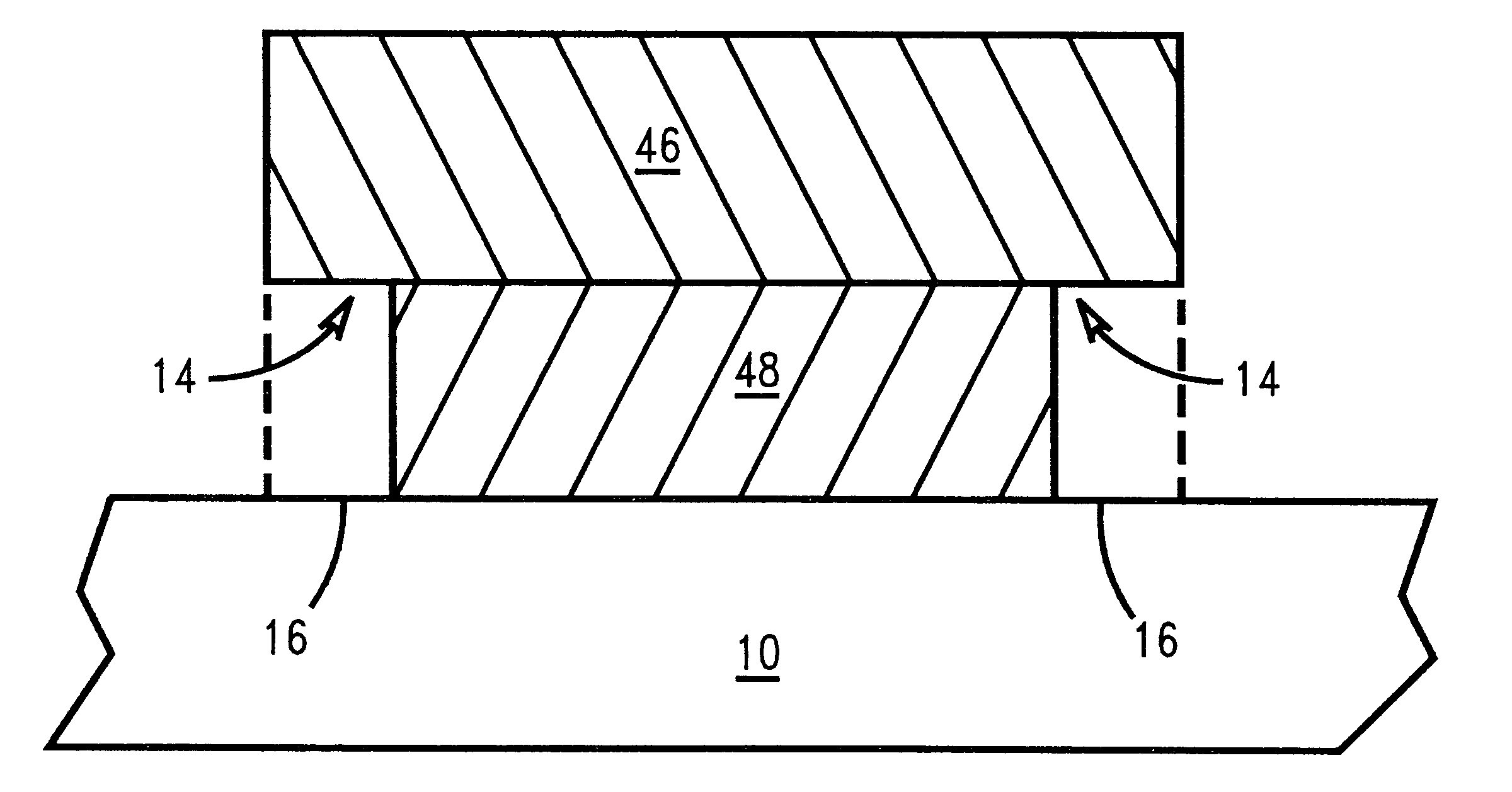
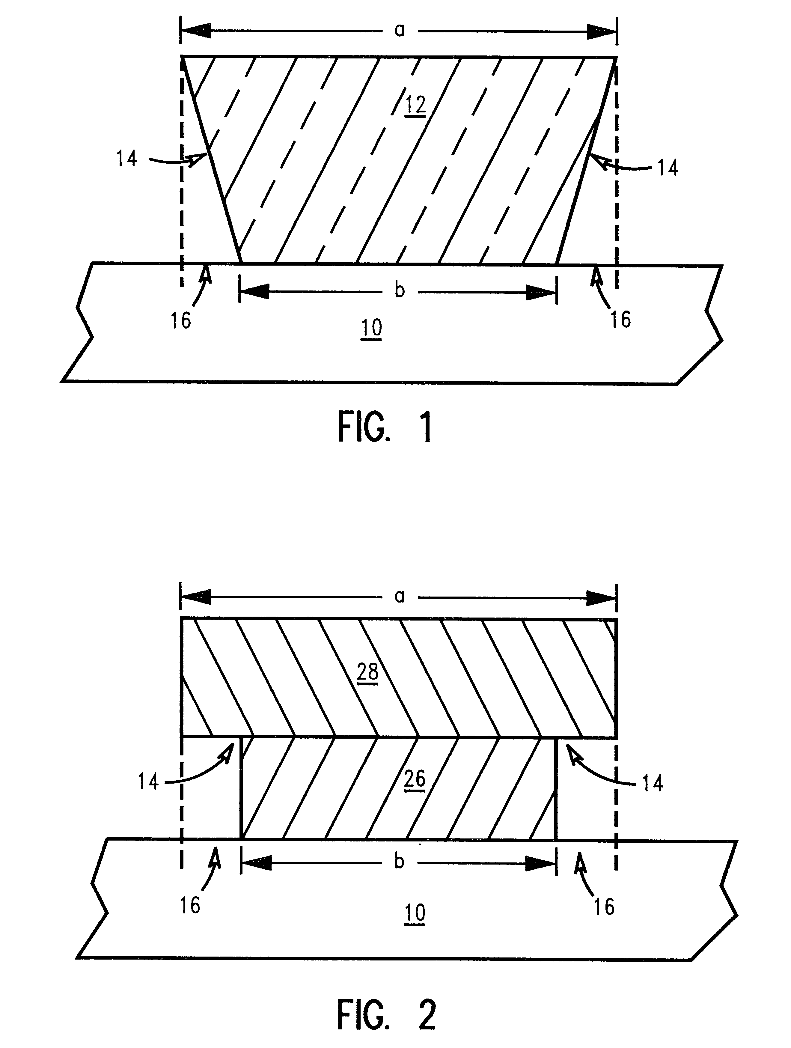
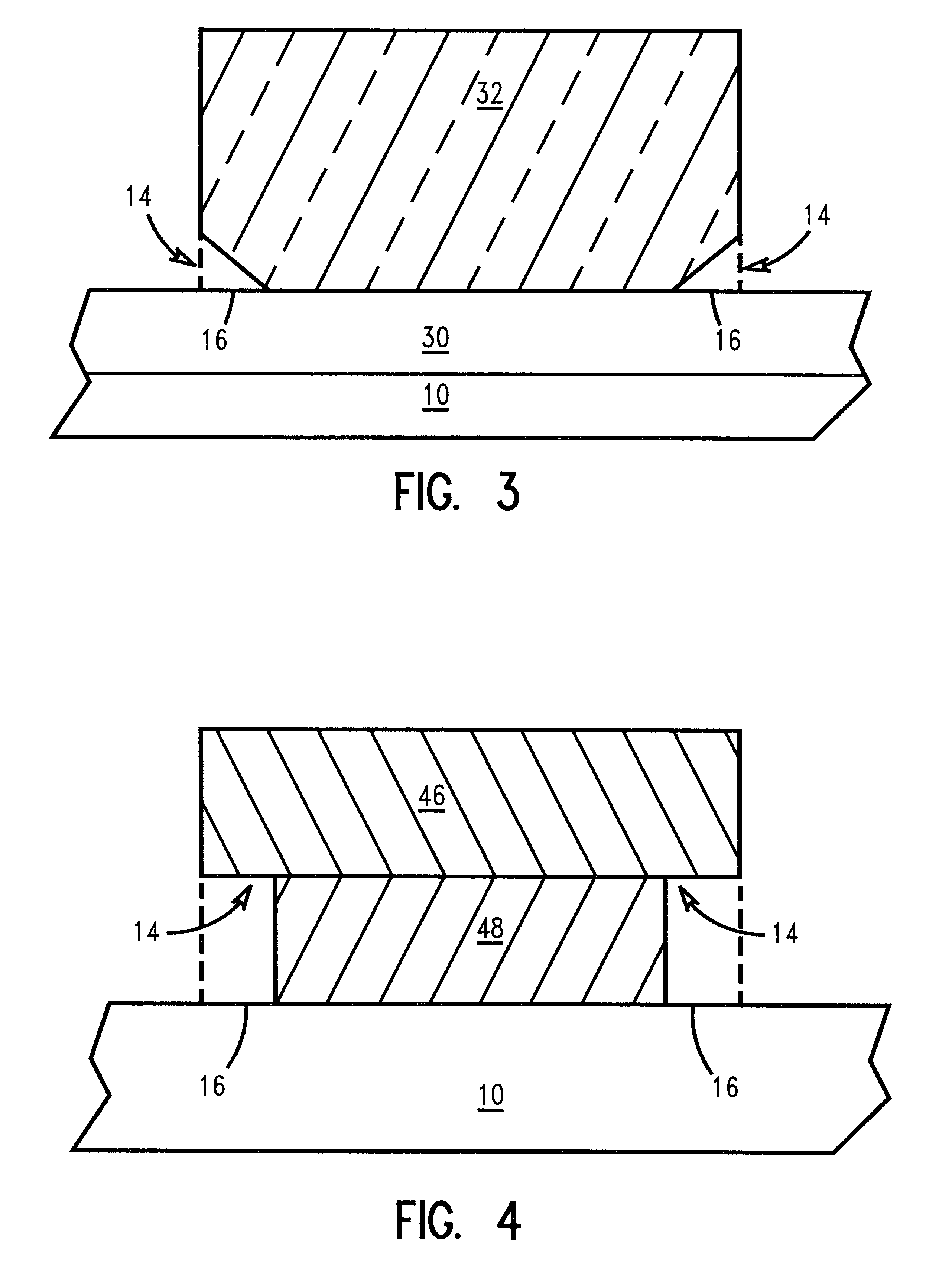
In describing the preferred embodiment of the present invention, reference will be made herein to FIGS. 1-4 of the drawings in which like numerals refer to like features of the invention. Features of the invention are not necessarily shown to scale in the drawings.

The present invention is directed to a method and process to reduce plasma etch fluting during the etching of a pattern on a substrate, such as a semiconductor substrate. The invention reduces fluting by forming a resist structure profile that is narrower at its base than the upper portion of the resist structure. The base of the resist structure is in contact with the surface of the substrate. The portion of the substrate that is adjacent to the base of the resist structure is "shadowed" or "shielded" from the primary etch direction by the wider upper portion of the resist structure. The wider portion of the resist structure is also referred to as an "overhang", or alternatively, an "undercut". The wider, upper portion o...


PUM

PropertyMeasurementUnit
thicknessaaaaaaaaaa
thicknessaaaaaaaaaa
thicknessaaaaaaaaaa

Abstract

The present invention is directed to a method and process to reduce plasma etch fluting during etching of a pattern on a semiconductor substrate by modifying the resist profile. The present invention forms a resist structure profile having an overhang or undercut, which is not in contact with the surface of the substrate. The overhang results in a shadowed region on the substrate from the primary etch direction adjacent to the base of the resist structure.Since the overhang is not in direct contact with the substrate surface, the resist pattern does not transfer into the surface of the substrate during etching and fluting is reduced or eliminated.

Description

1. Field of the InventionThe present invention relates generally to the etching of patterns on a semiconductor substrate and more specifically to a method and process to reduce plasma etch fluting during the etching of a pattern on a semiconductor substrate.2. Description of Related ArtModem oxide plasma etches based on fluorocarbon feed gases have a tendency to create fluted or scalloped profiles. Fluting is the creation of vertical sidewall irregularities during plasma etching, also referred to as striations, scalloping or sidewall roughness. The problem with the present art is that during etching, the pattern of the modified resist structure that is adjacent to the substrate is directly transferred into the surface of the substrate. The origin of the fluting appears to be a change in the structure of the resist mask during the etch by a combination of either polymer deposition or selective erosion. Fluting creates a number of problems including rough sidewalls, metallized ceramic...

Claims


Application Information

Patent Timeline
Patent Type & Authority Patents(United States)
IPC IPC(8): H01L21/70H01L21/84G03F7/095G03F7/38H01L21/027H01L21/308
CPCG03F7/095G03F7/38H01L21/0274H01L21/3085H01L21/3086Y10S438/942
Inventor BRUCE, JAMES A.BUSHEY, MARY C.JAGANNATHAN, PREMLATHA J.MLYRIKO, WALTER E.SUNDLING, DIANNE L.
Owner IBM CORP
Why Eureka
Try Eureka