Defect removable semiconductor devices
- Summary
- Abstract
- Description
- Claims
- Application Information
AI Technical Summary
Problems solved by technology
Method used
Image


Examples
Embodiment Construction
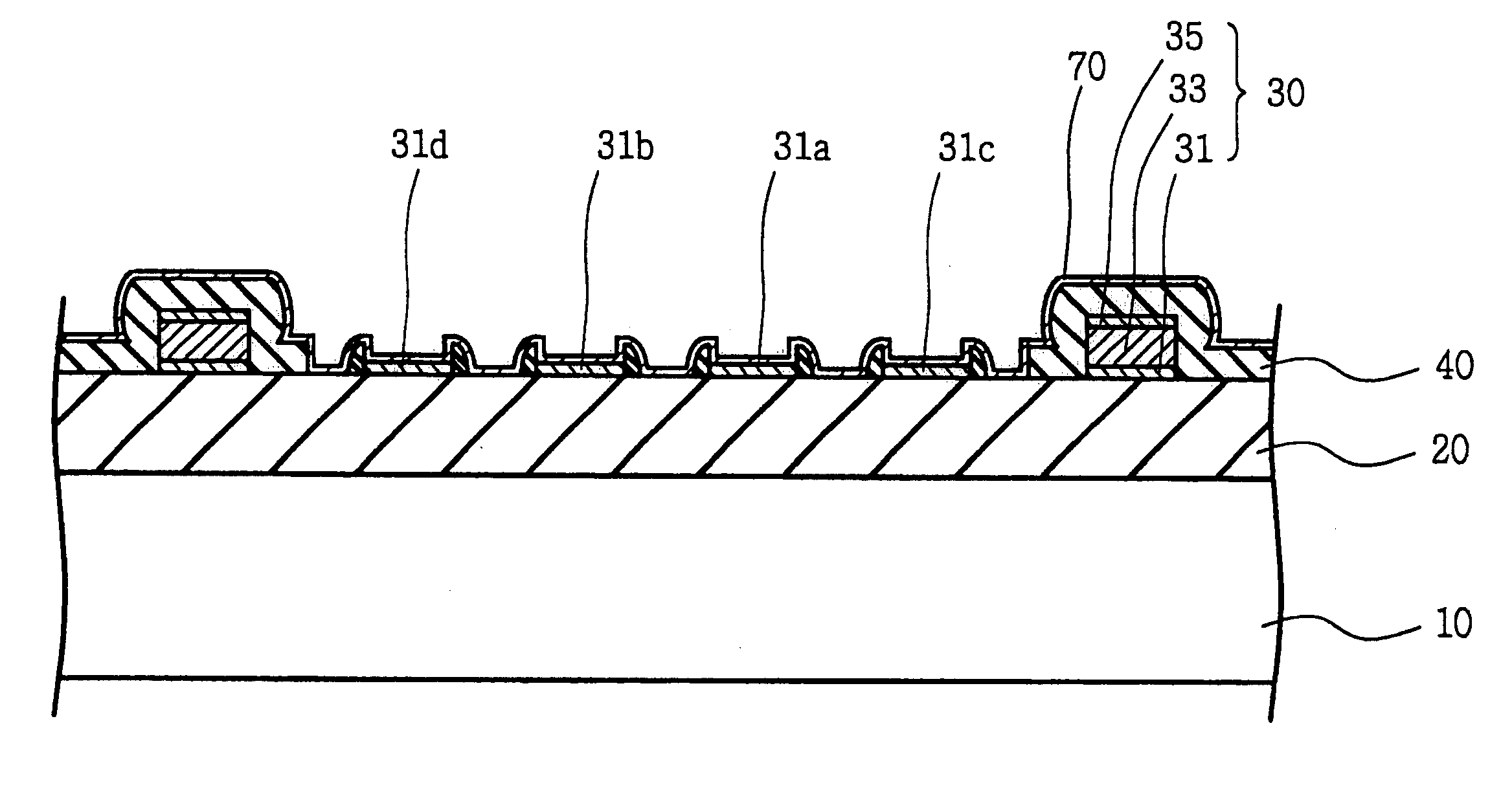
The structure of a defect removable semiconductor device and the manufacturing method thereof of the present invention will be described in detail with the accompanying drawings. FIG. 2 is a cross-sectional view for illustrating a defect removable semiconductor device in accordance with the present invention, and FIGS. 3 through 6 are diagrams for illustrating the manufacturing procedures of the defect removable semiconductor device. The same portions of the semiconductor device in the present invention will be referred by the same symbols used for as those in the conventional semiconductor element.
As shown in FIG. 2, an insulating interlayer 20 is deposited at respective regions of main memory cells and redundancy memory cells of a substrate 10. Final metal wires 30 are arranged on the insulating interlayer 20. A first protective layer 40 covers the insulating interlayer 20 including the metal wires 30 for protection.
The metal wire 30 is composed of a multi-layered structure having...
PUM
 Abstract
Description
Claims
Application Information
 - R&D
- Intellectual Property
- Life Sciences
- Materials
- Tech Scout
- Unparalleled Data Quality
- Higher Quality Content
- 60% Fewer Hallucinations
Browse by: Latest US Patents, China's latest patents, Technical Efficacy Thesaurus, Application Domain, Technology Topic, Popular Technical Reports.
© 2025 PatSnap. All rights reserved.Legal|Privacy policy|Modern Slavery Act Transparency Statement|Sitemap|About US| Contact US: help@patsnap.com