Fabrication of periodic surface structures with nanometer-scale spacings

a technology of periodic surface structure and nanometer-scale spacing, which is applied in the field of fabricating patterned crystals having two dimensionally periodic surface structures, can solve the problems of difficult to produce dimensions on a length-scale of less than 100 nm using these techniques, and the significant amount of instrumental evolution that needs to take pla

Inactive Publication Date: 2001-12-11
CORNELL RES FOUNDATION INC
View PDF5 Cites 47 Cited by
  • Summary
  • Abstract
  • Description
  • Claims
  • Application Information

AI Technical Summary

Problems solved by technology

Unfortunately, previously known techniques for forming nanometer-scale patterns are not commercially feasible.
However, producing dimensions on a length-scale of less than 100 nm using these techniques is difficult and can be carried out only using very special imaging tools and materials.
However, there is a significant amount of instrumental evolution that needs to take place before these proximal probe techniques can be practical in a high throughput environment.
At small misorientation angles, these stress and strain fields result from the presence of crystal defects, known as dislocations, at the interface between the crystals.

Method used


Image

  • Fabrication of periodic surface structures with nanometer-scale spacings
  • Fabrication of periodic surface structures with nanometer-scale spacings
  • Fabrication of periodic surface structures with nanometer-scale spacings

Examples


Embodiment Construction

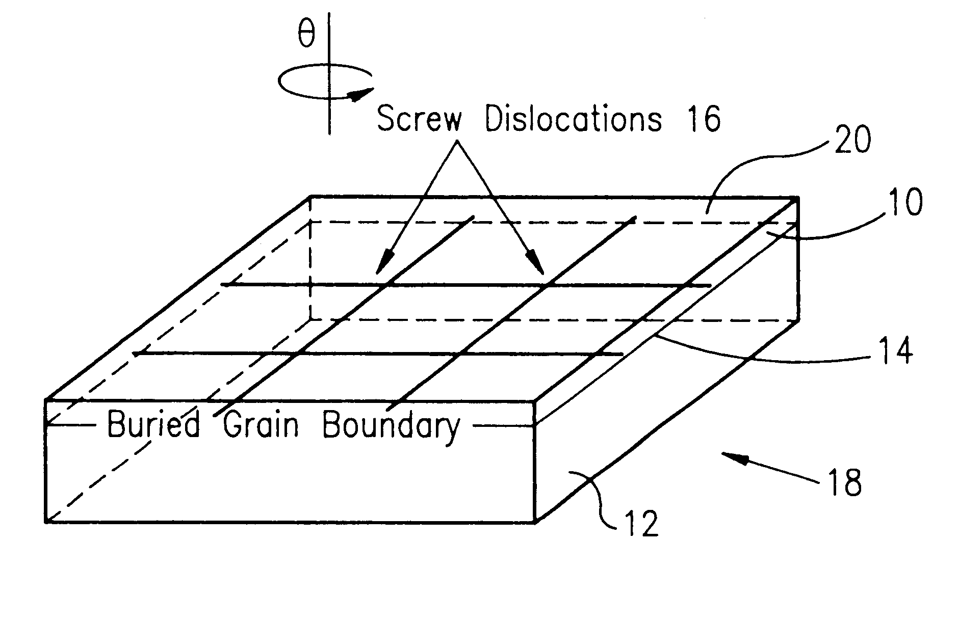
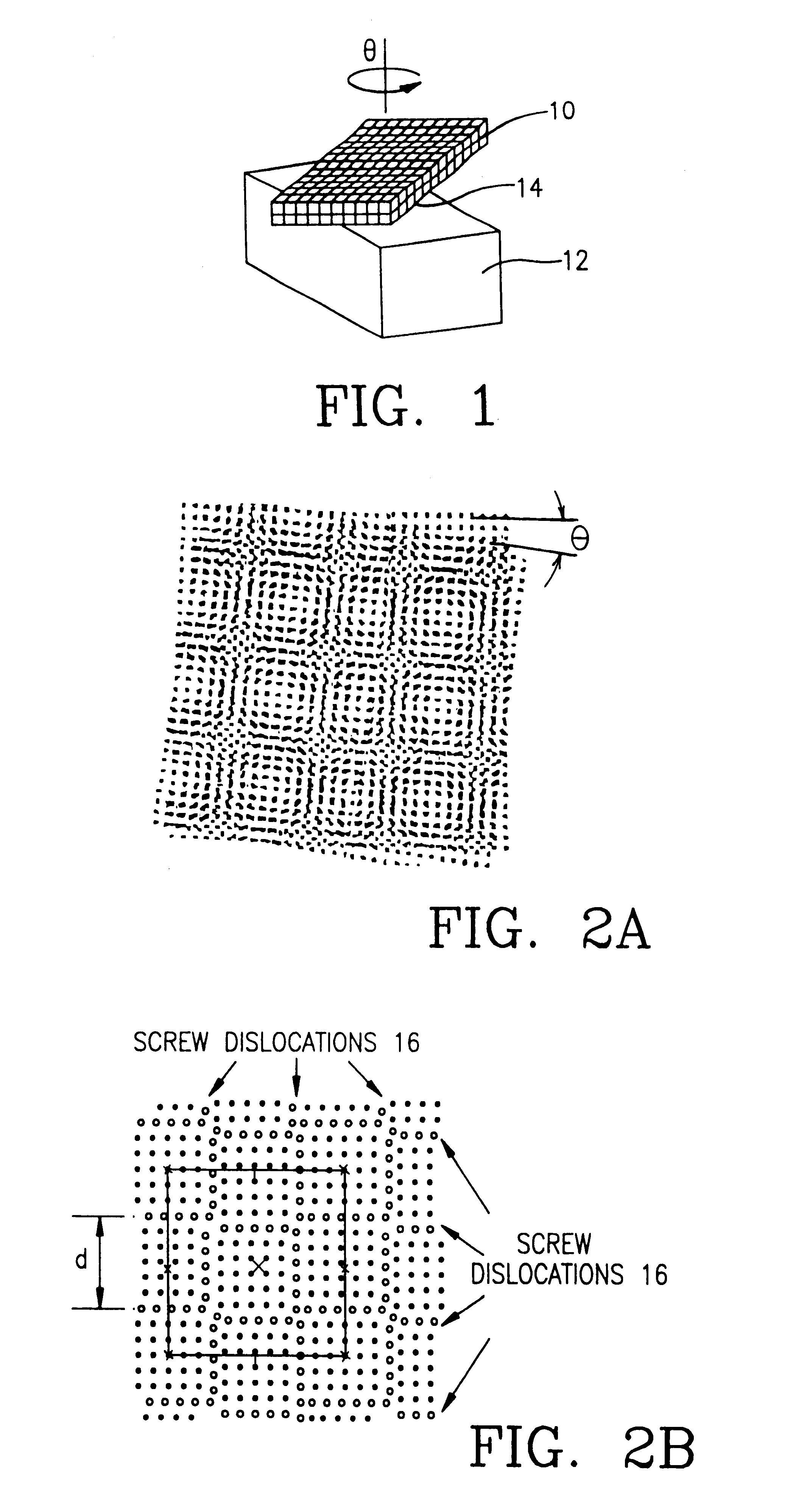
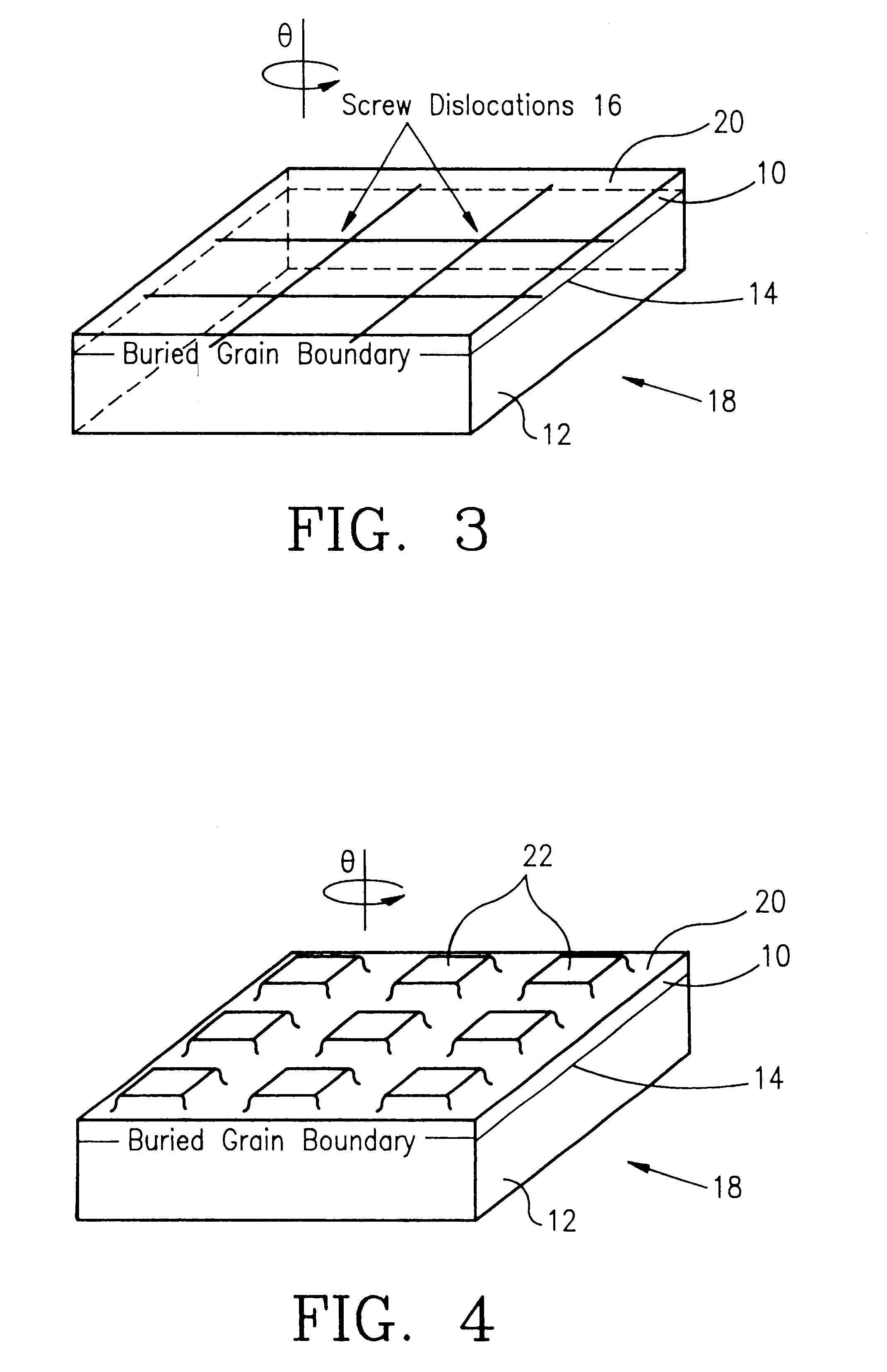
Turning now to a more detailed consideration of a preferred embodiment of the present invention, FIG. 1 illustrates the geometry associated with the twist bonding of a first, thin (001) single crystal 10 to a second, bulk (001) single crystal 12 misoriented by an angle .theta. about a common normal with respect to one another, thereby creating a twist grain boundary 14 between the two crystals 10 and 12. A twist grain boundary is a grain boundary between two crystals that have the same surface normal and are rotated with respect to one another about this normal.

With reference to FIGS. 2A and 2B, when the two single crystals 10 and 12 are initially brought into contact, a misfit exists between the two lattices along the boundary plane if no structural relaxation occurs. FIG. 2A shows the Moire pattern created by the two planes of atoms immediately adjacent to the grain boundary with no relaxation. This configuration is a high-energy state due to the high distortion in the atomic bond...


PUM

PropertyMeasurementUnit
thicknessaaaaaaaaaa
thicknessaaaaaaaaaa
thicknessaaaaaaaaaa

Abstract

The periodic stress and strain fields produced by a pure twist grain boundary between two single crystals bonded together in the form of a bicrystal are used to fabricate a two-dimensional surface topography with controllable, nanometer-scale feature spacings (e.g., from 50 nanometers down to 1.5 nanometers). The spacing of the features is controlled by the misorientation angle used during crystal bonding. One of the crystals is selected to be thin, on the order of 5-100 nanometers. A buried periodic array of screw dislocations is formed at the twist grain boundary. To bring the buried periodicity to the surface, the thin single crystal is etched to reveal an array of raised elements, such as pyramids, that have nanometer-scale dimensions. The process can be employed with numerous materials, such as gold, silicon and sapphire. In addition, the process can be used with different materials for each crystal such that a periodic array of misfit dislocations is formed at the interface between the two crystals.

Description

1. Field of the InventionThe present invention relates in general to a technique for fabricating patterned crystals having two dimensionally periodic surface structures with nanometer-scale spacings.2. Description of the Background ArtAs the demand for smaller and smaller electronic devices, magnetic recording media, etc., has increased, a need has been created for improved fabrication processes for making such devices. Many such devices are or can be typically formed on substrates that have two-dimensional patterns of periodic surface structures that are used for the subsequent formation of the devices. The reduced size demands for the devices require that the spacings between the periodic structures be on the order of less than 100 nm. Unfortunately, previously known techniques for forming nanometer-scale patterns are not commercially feasible. For example, a number of lithographic methods exist that can be used to form these types of patterned structures. These methods include cr...

Claims


Application Information

Patent Timeline
Patent Type & Authority Patents(United States)
IPC IPC(8): C30B33/00C30B33/06G11B5/84H01F1/00H01F41/30H01F41/14G11B5/00G11B5/74B82B3/00B82B1/00G11B5/65
CPCB82Y25/00C30B33/00C30B33/06G11B5/84H01F1/009H01F41/30B82Y40/00C30B29/605Y10T428/12472G11B5/74G11B2005/0002Y10T428/12646Y10S428/926Y10S117/902Y10T428/12674Y10T428/12993Y10T428/12889
Inventor SASS, STEPHEN L.OBER, CHRISTOPHER K.SUZUKI, YURI
Owner CORNELL RES FOUNDATION INC
Why Eureka
Try Eureka