Method and apparatus for three dimensional interconnect analysis

a three-dimensional interconnect and analysis method technology, applied in the field of three-dimensional interconnect analysis, can solve the problems of increasing the dominance of the rc delay in the on-chip signal delay, exceedingly small switching time of transistors, and increasing the performance of the on-chip circui

Inactive Publication Date: 2001-12-11
SIMPLEX SOLUTIONS INC
View PDF15 Cites 29 Cited by
  • Summary
  • Abstract
  • Description
  • Claims
  • Application Information

AI Technical Summary

Problems solved by technology

As the feature size of advanced integrated circuits continues to decrease and transistor switching times become ever shorter, on-chip signal delay is increasingly dominated by the RC delay associated with the signal lines.
With recent advances in chip technology, the switching time of transistors has become exceedingly small.
As a result, the performance of on-chip circuits has become increasingly limited by the RC delay associated with signal lines.
However, they are severely limited in the variety of geometries that can be analyzed, and are incapable of handling the geometries typical of advanced chips and packages.
Approximate formulas based on anything other than detailed numerical solution or hardware measurement are incapable of producing sufficiently accurate capacitance values for advanced chips and packages.
However because the conductor net geometry is dissimilar to the patterns, the pattern fields cannot be superimposed, which introduces a nonlinear geometrical error.
As a result, 2D and 2.5D algorithms that use simple patterns are inherently inaccurate.
All of these faults show that 2D and 2.5D algorithms arc not suitable to extract high accuracy capacitance and resistance models.
The finite-element and finite-difference methods have the disadvantage that they must fill all space with a 3D volume discretization or grid.
Typically, finite-element methods require an extremely large number of unknowns to obtain acceptable accuracy.
As a result, using the finite-element method and finite-difference method are not feasible for large models.
Simulating multiple dielectrics is not straightforward with boundary integral methods utilizing single integrals since these only solve for the unknown charge density and not the required potential on the dielectric boundaries.
The disadvantage of the boundary integral equation method is that the matrix of coefficients of the linear system is dense, and each individual matrix element is costly to evaluate.
As a result, using the boundary integral equation method is not feasible for large models.
These methods generate a single capacitance value for a conductor independent of available simulation time, and therefore cannot refine or provide a more accurate solution if desired.

Method used


Image

  • Method and apparatus for three dimensional interconnect analysis
  • Method and apparatus for three dimensional interconnect analysis
  • Method and apparatus for three dimensional interconnect analysis

Examples


Embodiment Construction

The preferred embodiment of the present invention will be discussed with reference to the accompanying drawings. In the following description, numerous specific details are set forth in order to provide a thorough understanding of the present invention. It will be obvious, however, to those skilled in the art that the present invention may be practiced without these specific details. In other instances, well-known structures are not shown in detail in order to avoid unnecessarily obscuring the present invention.

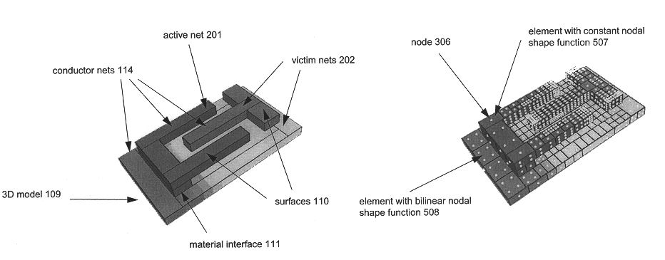
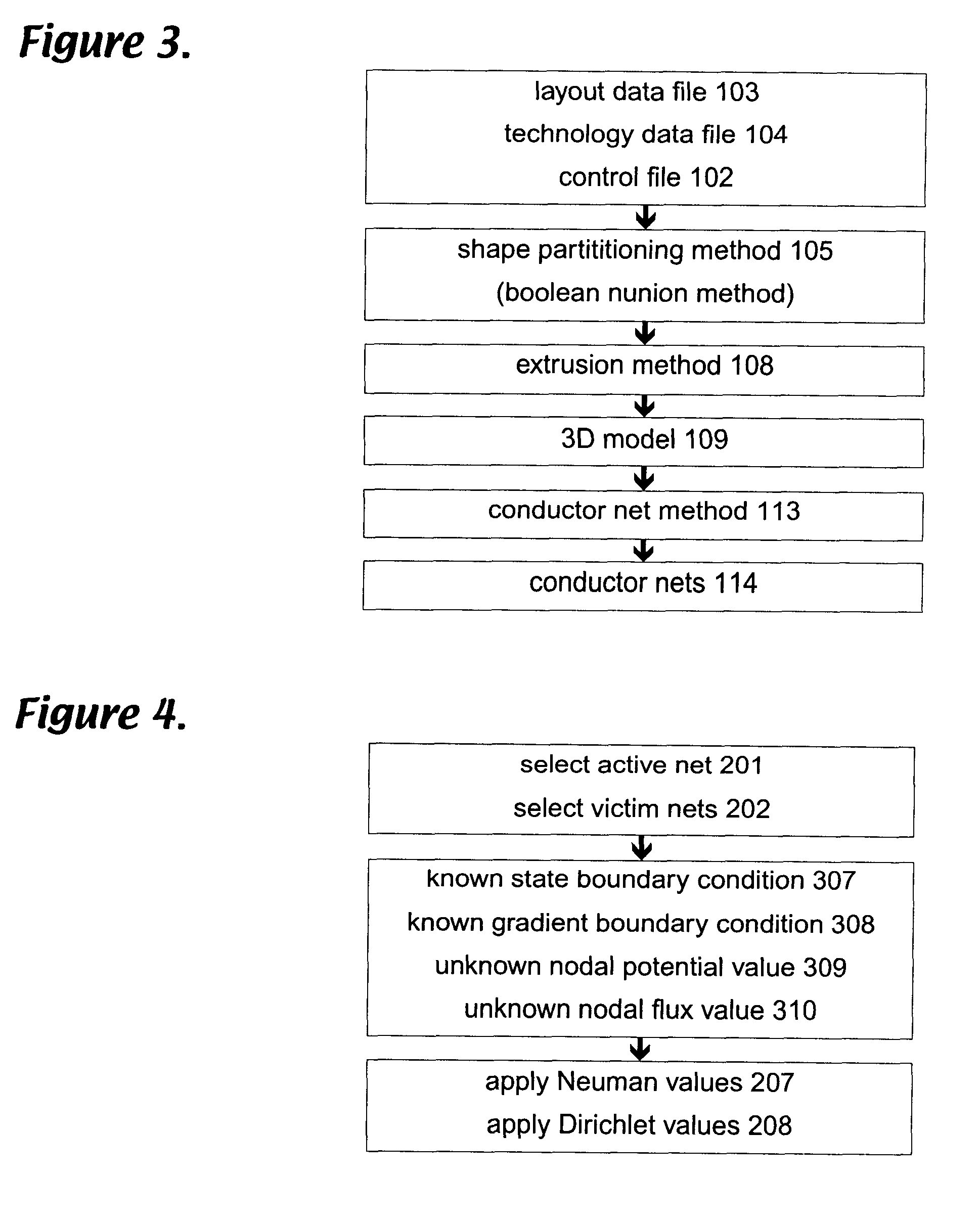
FIG. 2 is a block diagram showing a construction of the interconnect analysis method according to the present invention. First a geometry generating method 100 reads an input circuit description and creates a 3D model 109 (shown in FIGS. 3, 12). A conductor net method is thus applied to the model to identify a plurality of electrically connected conductor nets 114 (also shown in FIGS. 3, 12). Next a boundary condition application method 200 applies appropriate Neuman and Diri...


PUM


Abstract

A method for calculating the parasitic capacitance and resistance in a semiconductor device is disclosed. According to the preferred embodiment, a layout file containing the shapes of semiconductor interconnects and a technology file describing the fabrication steps are used to generate a 3D model of the structures. The surfaces of the model are discretized and a double boundary integral equation is solved to compute the field allowing various interconnect parameters to be computed, including resistance, self-capacitance, cross-capacitance, and current density. Further, the preferred embodiment discloses how numerical analysis can be efficiently performed on typical large interconnect and substrate structures.

Description

1. Field of the InventionThis invention relates to a method for deriving the parasitic parameters of conductors. More specifically, the invention relates to a method for calculating the capacitance between conductors and resistance in conductors in an integrated circuit.2. Description of the Related ArtAs the feature size of advanced integrated circuits continues to decrease and transistor switching times become ever shorter, on-chip signal delay is increasingly dominated by the RC delay associated with the signal lines. In order for circuits to produce meaningful and reliable results, the circuit models used must include accurate values for the capacitances and resistances of the signal lines. The complex dielectric structures present in advanced chip and package technologies can have a substantial effect on the signal line capacitance values. The only practical method for obtaining accurate capacitance values for such geometries is detailed numerical solution.In the electrical mod...

Claims


Application Information

Patent Timeline
Patent Type & Authority Patents(United States)
IPC IPC(8): G06F17/50
CPCG06F17/5018G06F30/23
Inventor LJUNG, PERBACHTOLD, MARTIN
Owner SIMPLEX SOLUTIONS INC
Why Eureka
Try Eureka