Chemical mechanical polishing in-situ end point system

a technology of end point system and mechanical polishing, which is applied in the direction of grinding machine components, manufacturing tools, lapping machines, etc., can solve the problems of large wafer destruction, item being polished may have to be scrapped, and item not being properly planarized,

Inactive Publication Date: 2002-01-01
GLOBALFOUNDRIES INC
View PDF19 Cites 112 Cited by
  • Summary
  • Abstract
  • Description
  • Claims
  • Application Information

AI Technical Summary

Problems solved by technology

If too much material is removed the item being polished may have to be scrapped.
If too little material is removed, the item will not be properly planarized and must be reworked/repolished.
However, such conventional systems often destroy large numbers of wafe

Method used


Image

  • Chemical mechanical polishing in-situ end point system
  • Chemical mechanical polishing in-situ end point system
  • Chemical mechanical polishing in-situ end point system

Examples


Embodiment Construction

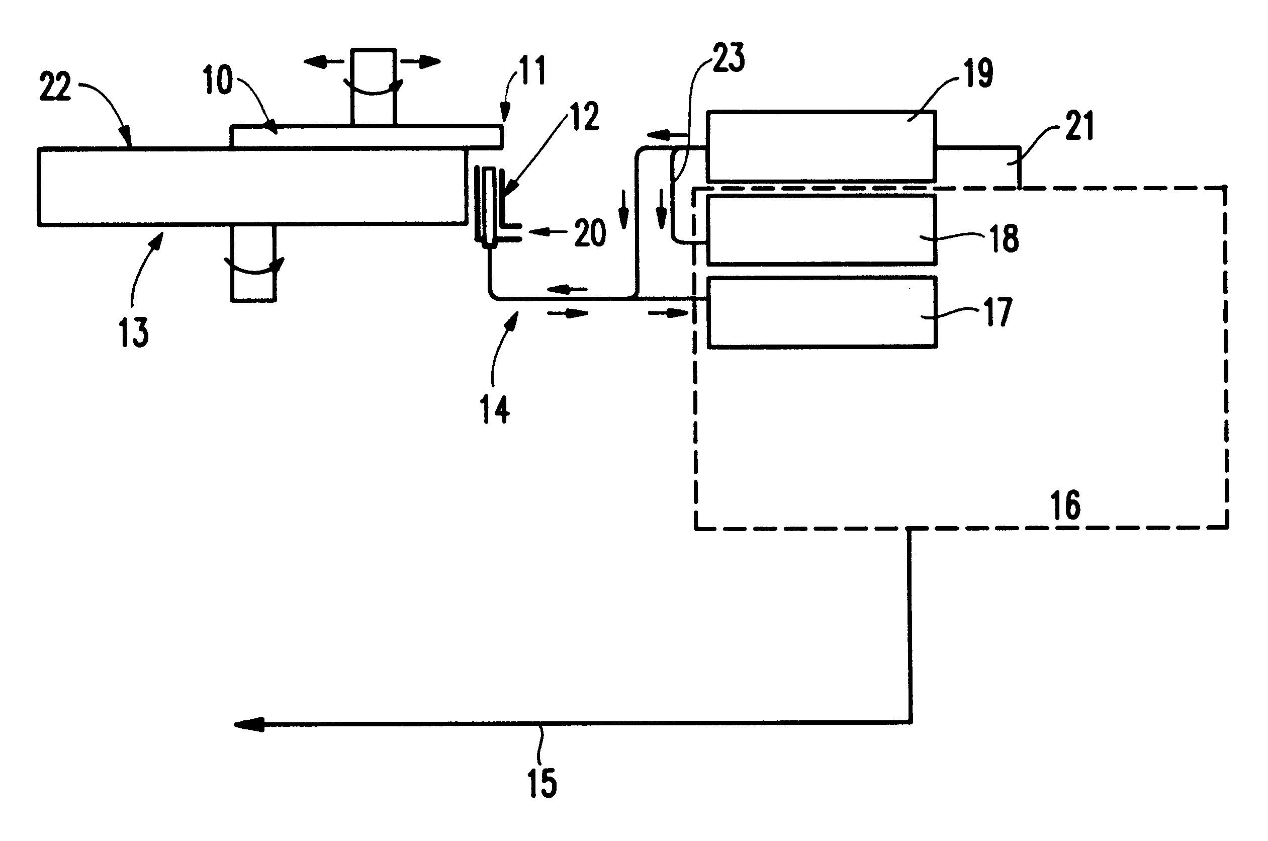
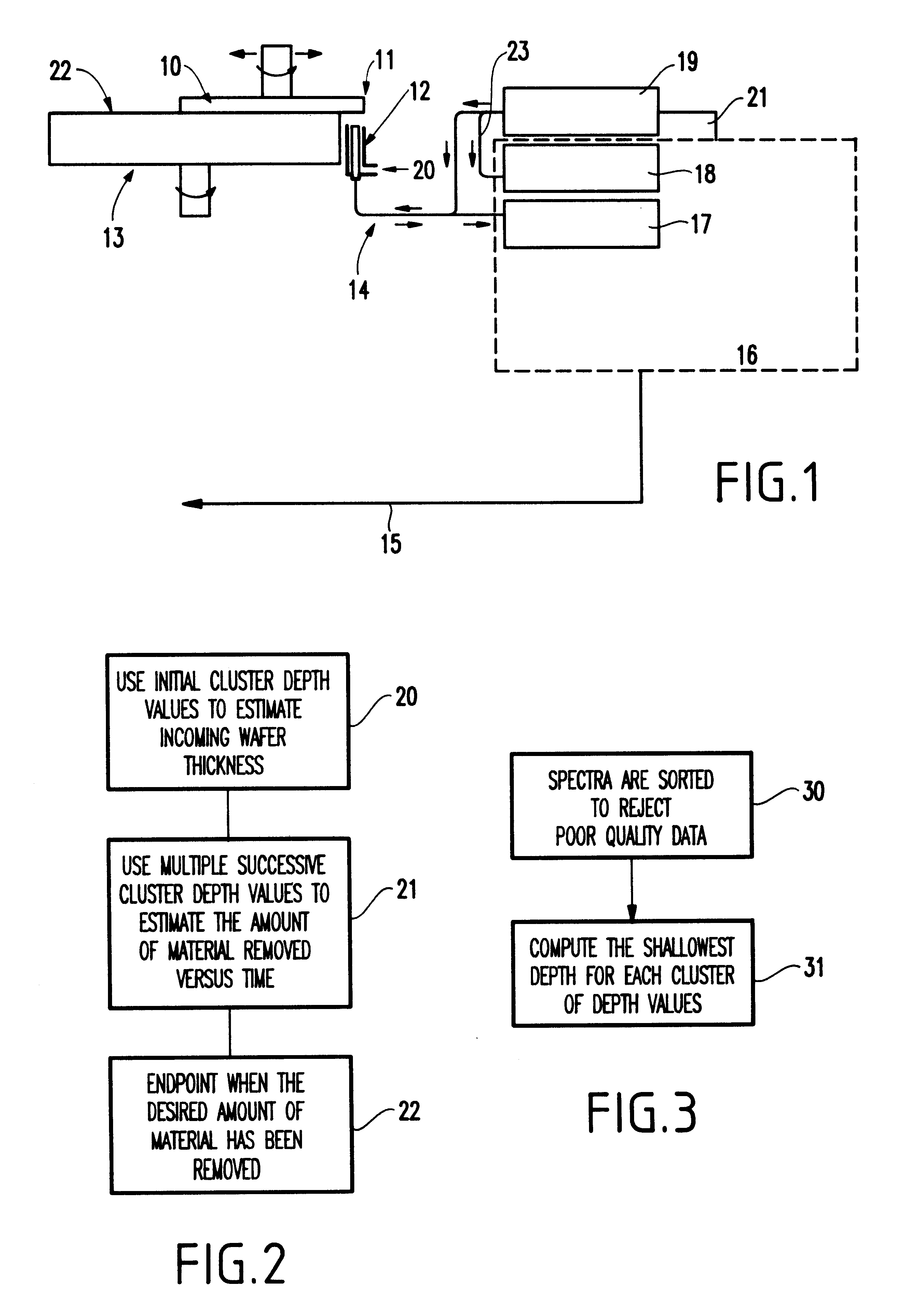
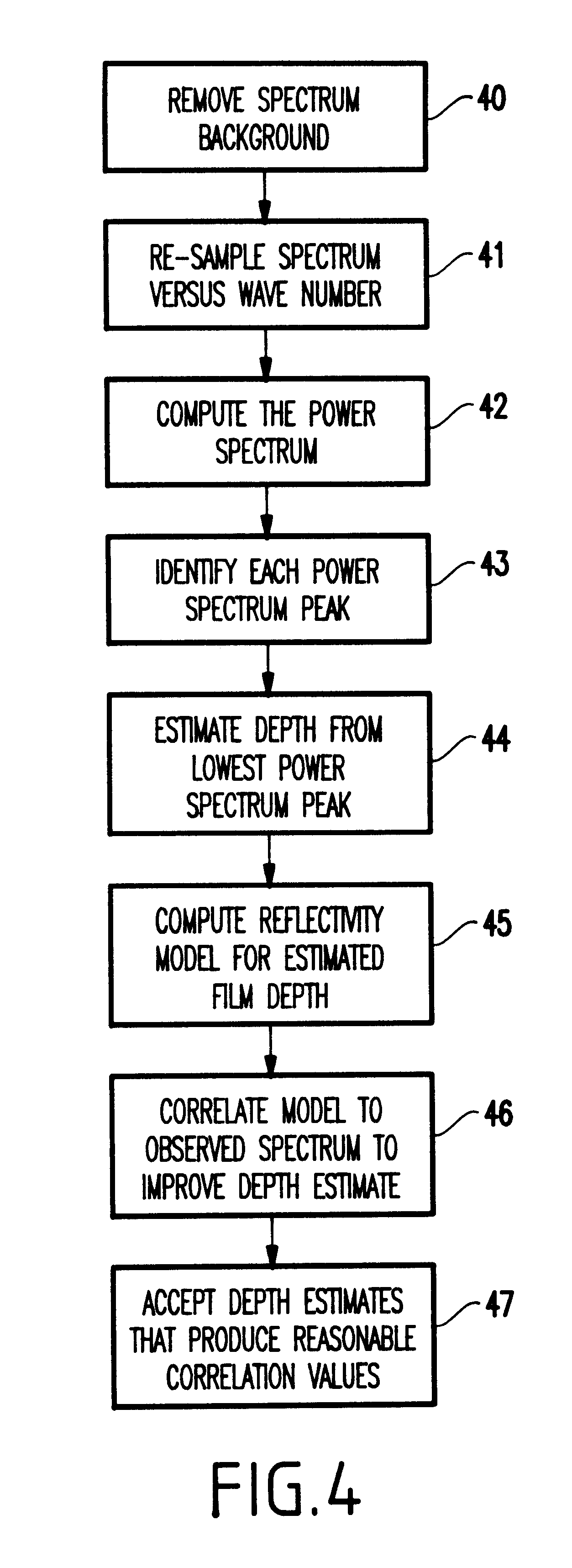
The invention uses optics to achieve an endpoint signal that eliminates the need for send-ahead measurements. Thus, the invention is capable of screening catastrophic failure conditions to eliminate silent failures that would otherwise cause large scale product scrap conditions. The invention can be used with any polishing system (e.g., a chemical mechanical polishing (CMP) system), such as systems for removing transparent films or systems for removing non-transparent films. The invention is not limited to polishing any specific type of device but instead is applicable to polishing or planarizing any surface. Therefore, for example, the invention could be utilized to polish any material to a given thickness, such as optical devices, glasses, metals, integrated circuit wafers or any surface with one or more semi-transparent films.

FIG. 1 illustrates a preferred embodiment of the invention. The invention includes means for polishing which applies an abrasive to an item being polished. ...


PUM


Abstract

A structure and method for polishing a device include oscillating a carrier over an abrasive surface (the carrier bringing a polished surface of the device into contact with the abrasive surface, the oscillating allowing a portion of the polished surface to periodically oscillate off the abrasive surface), optically determining a reflective measure of a plurality of locations of the polished surface as the portion of the device oscillates off the abrasive surface and calculating depths of the locations of the polished surface based of the reflective measure.

Description

1. Field of the InventionThe present invention generally relates to planarizing systems and more particularly to an improved chemical mechanical polishing system with real-time polishing rate measurement and control.2. Description of the Related ArtChemical mechanical polishing / planarization (CMP) is becoming more popular as a choice for planarizing materials in today's advanced integrated circuit devices. More specifically, the increased use of shallow trench isolation (STI) regions makes chemical mechanical polishing a more commonly used process.Basically, in a chemical mechanical polishing process a surface of an item, such as a wafer, is made planar (e.g., substantially flat) by holding the wafer (e.g., using a rotating carrier) against a rotating polishing table that contains an abrasive slurry. Material is removed to render the exposed surface planar. The rate that the material is removed from the wafer depends upon the pressure applied between the carrier and the polishing ta...

Claims


Application Information

Patent Timeline
IPC IPC(8): B24B37/04B24B49/04B24B49/02B24B49/12B24B37/013H01L21/304
CPCB24B37/013B24B49/12B24B49/04
Inventor LEBEL, RICHARD J.NADEAU, ROCKO'BOYLE, MARTIN P.SMITH, JR., PAUL H.VAN KESSEL, THEODORE G.WICKRAMASINGHE, HEMANTHA K.
Owner GLOBALFOUNDRIES INC
Why Eureka
Try Eureka