Plasma display panel with dielectric layer suppressing reduced electrode conductivity

a dielectric layer and display panel technology, applied in the manufacture of electrode systems, electric discharge tubes/lamps, instruments, etc., can solve the problems of difficult drive of pdp and rise of resistance of transparent electrodes, and achieve the effect of reducing conductivity

Inactive Publication Date: 2002-02-05
HITACHT MAXELL LTD
View PDF11 Cites 22 Cited by
  • Summary
  • Abstract
  • Description
  • Claims
  • Application Information

AI Technical Summary

Benefits of technology

In view of the foregoing, it is an object of the present invention to provide a plasma display panel and method of manufacturing it whereby the rise of resistance of the transparent electrodes can be prevented.
A further object of the present invention is to provide a plasma display panel and method of manufacturing it whereby the sustaining discharge voltage can be kept low by lowering the resistance of the transparent electrodes.
Further, in another invention, the main constituent of the transparent electrode is indium oxide and indium oxide is included in the dielectric layer. By including the main constituent of the transparent electrodes in the dielectric layer, it is believed that the drop in conductivity caused by diffusion of the dielectric substance in the transparent electrodes during high-temperature processing is prevented.

Problems solved by technology

In this high-temperature firing step, or due to high temperature in subsequent operation, there is the problem that the resistance of the transparent electrodes rises.
Such rise in the resistance of the transparent electrodes causes in particular a rise in the sustaining discharge voltage between transparent electrode pairs, making drive of the PDP difficult.

Method used


Image

  • Plasma display panel with dielectric layer suppressing reduced electrode conductivity
  • Plasma display panel with dielectric layer suppressing reduced electrode conductivity
  • Plasma display panel with dielectric layer suppressing reduced electrode conductivity

Examples


Embodiment Construction

Embodiments of the present invention are described below with reference to the drawings. However, these embodiments are not limitative of the technical scope of the present invention.

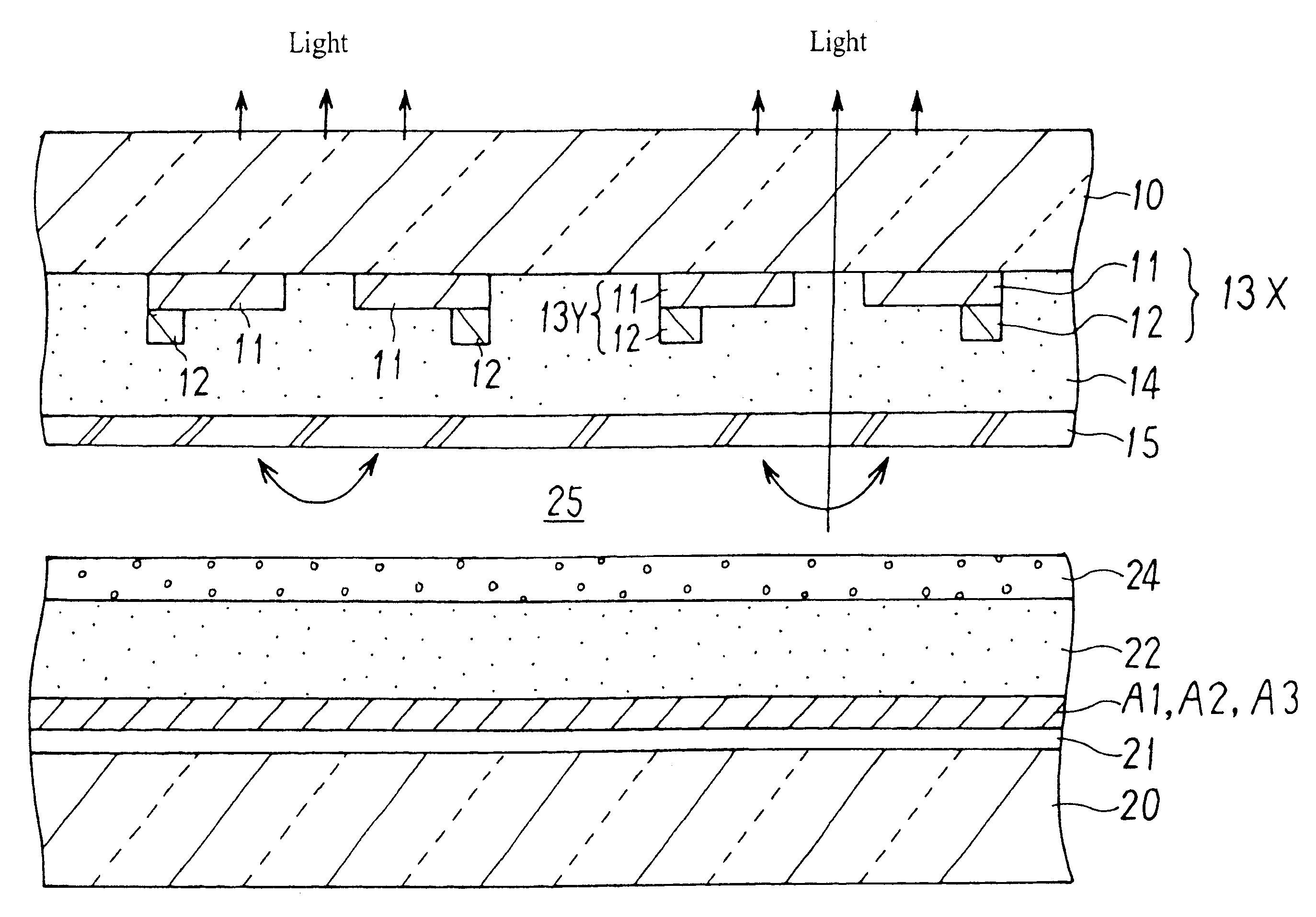
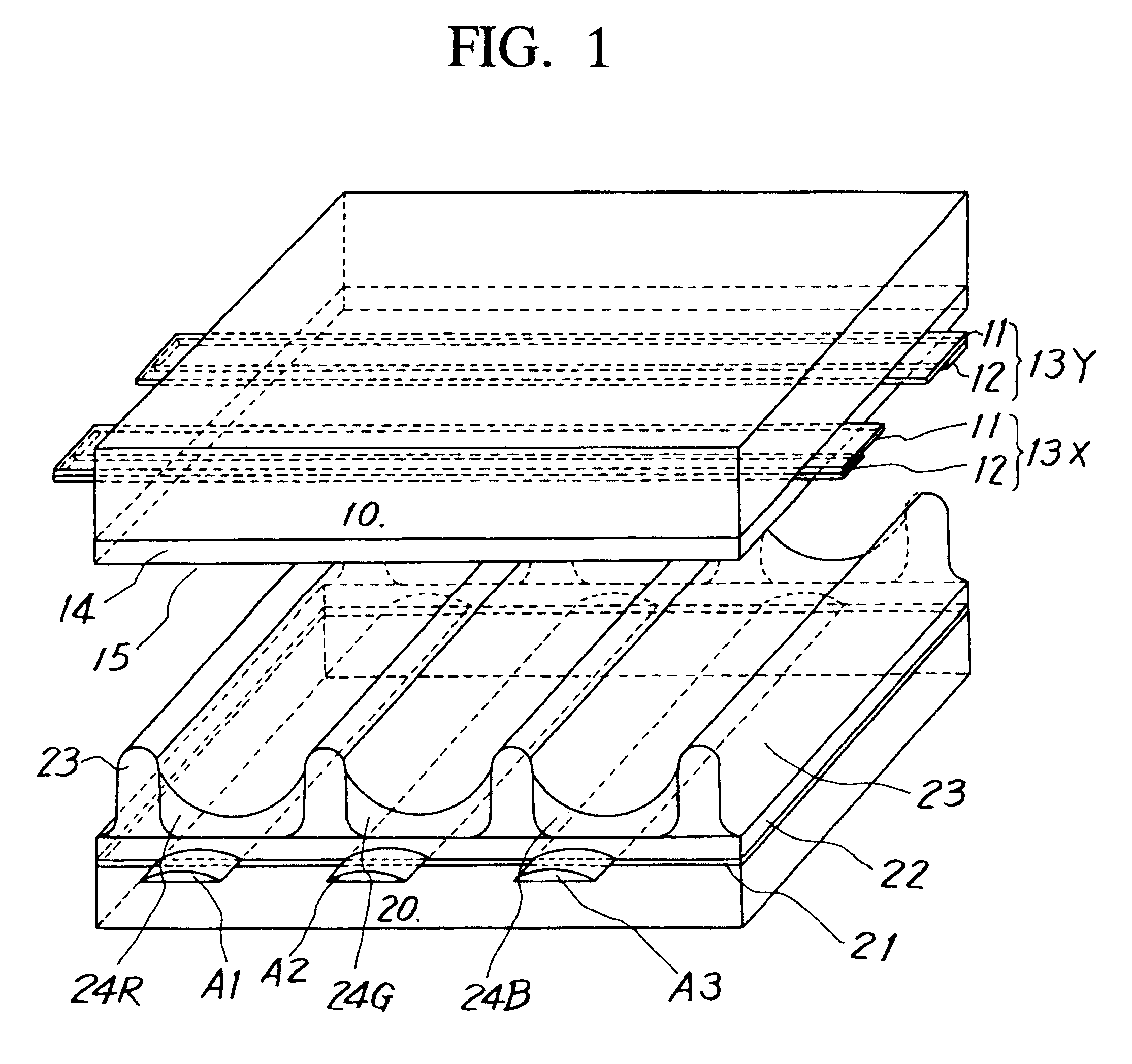
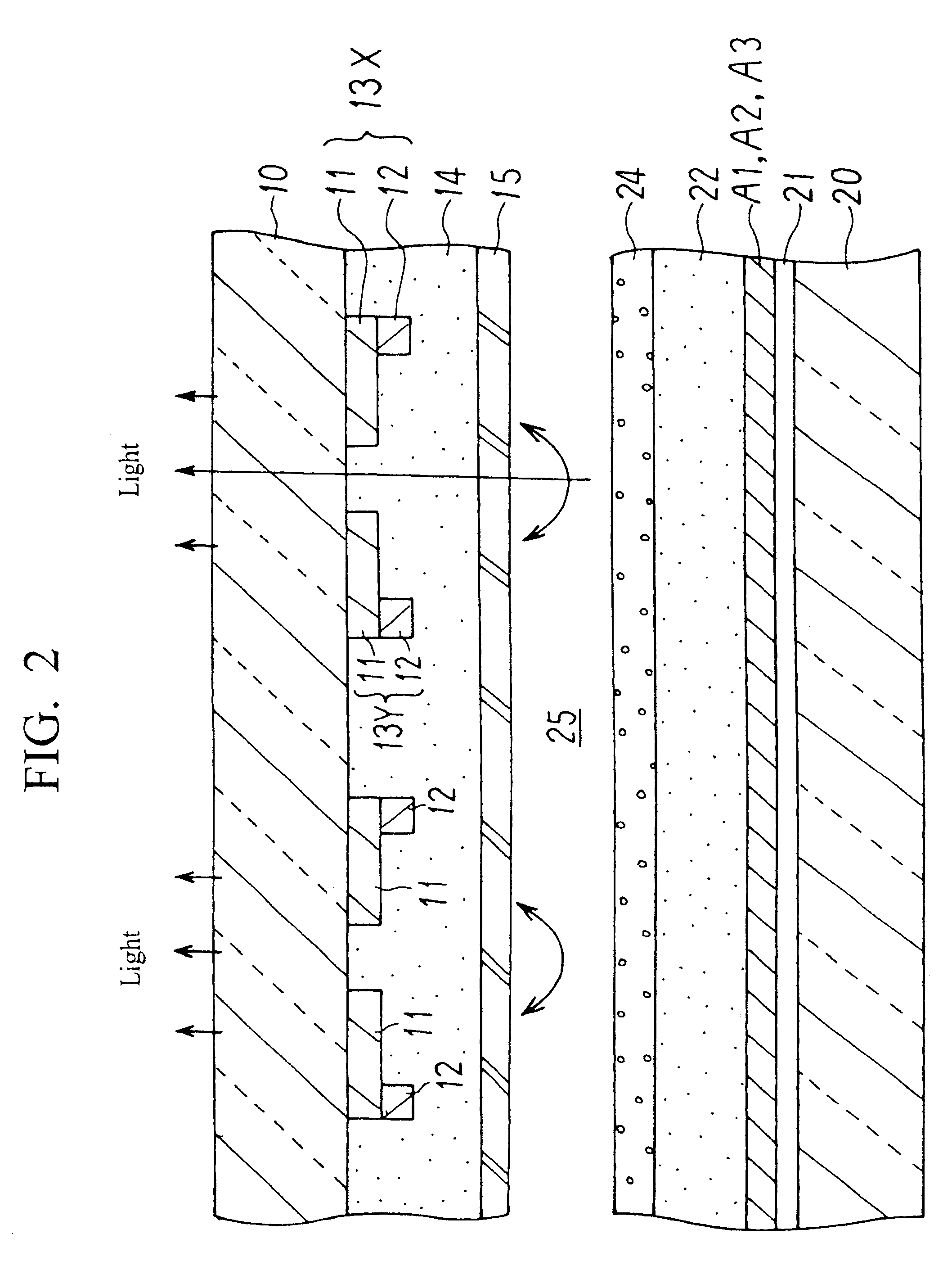
FIG. 1 is an exploded perspective view of an AC type PDP of the three-electrode surface discharge type according to an embodiment of the present invention. FIG. 2 is a cross-sectional view of this PDP. The construction will be described with reference to both drawings. In this example, the display light issues in the direction (direction shown in FIG. 2) of the display-side glass substrate 10. 20 is the rear-face glass substrate. On the display-side glass substrate 10, there are formed X electrodes 13X and Y electrodes 13Y comprising transparent electrodes 11 and bus electrodes 12 of high electrical conductivity formed thereon (below in the drawing). These electrode pairs are covered by a dielectric layer 14 and protective layer 15 consisting of MgO. Bus electrodes 12 are provided along opposite edges o...


PUM

PropertyMeasurementUnit
voltageaaaaaaaaaa
temperatureaaaaaaaaaa
transparentaaaaaaaaaa

Abstract

The present invention relates to a plasma display panel comprising transparent electrodes and a dielectric layer covering said transparent electrodes on at least one substrate of a pair of substrates facing each other with a discharge space therebetween, the main constituent of the transparent electrodes is included in the dielectric layer. Further, the main constituent of the transparent electrode is indium oxide and indium oxide is included in the dielectric layer. By including the main constituent of the transparent electrodes in the dielectric layer, it is believed that the drop in conductivity caused by diffusion of the dielectric substance in the transparent electrodes during high-temperature processing is prevented.

Description

BACKGROUND OF THE INVENTION1. Field of the InventionThe present invention relates to plasma display panels and a method of manufacturing them, and in particular relates to the dielectric layer covering the transparent electrodes.2. Description of the Related ArtPlasma display panels (hereinbelow abbreviated to PDP) have attracted attention as large-screen full color display devices. In particular, in a three-electrode surface discharge type AC type PDP, a plurality of display electrode pairs that generate surface discharges are formed on a display side substrate. Address electrodes orthogonal to these display electrodes and a phosphor layer covering these are formed on a rear face substrate. The fundamental basis of driving a PDP is that a large voltage is supplied to the display electrode pairs to effect resetting. A discharge is generated between one electrode of an electrode pair and an address electrode, and a sustaining discharge is generated by applying a sustaining voltage ac...

Claims


Application Information

Patent Timeline
Patent Type & Authority Patents(United States)
IPC IPC(8): G06F17/50C03C3/04H01J9/02H01J11/12H01J11/14H01J11/22H01J11/24H01J11/26H01J11/28H01J11/34H01J11/36H01J11/38H01J11/42
CPCG06F17/5022G06F30/33C03C3/04
Inventor AWAJI, NORIYUKIBETSUI, KEIICHITADAKI, SHINJI
Owner HITACHT MAXELL LTD
Why Eureka
Try Eureka