

Impedance conversion circuit
a technology of impedance conversion and circuit, which is applied in the direction of impedence convertors, power conversion systems, instruments, etc., can solve the problems of difficult to develop digital processing, inability to achieve desired filter transmission characteristics, and inability to perform analog processing
- Summary
- Abstract
- Description
- Claims
- Application Information
AI Technical Summary
Problems solved by technology
Method used
Image

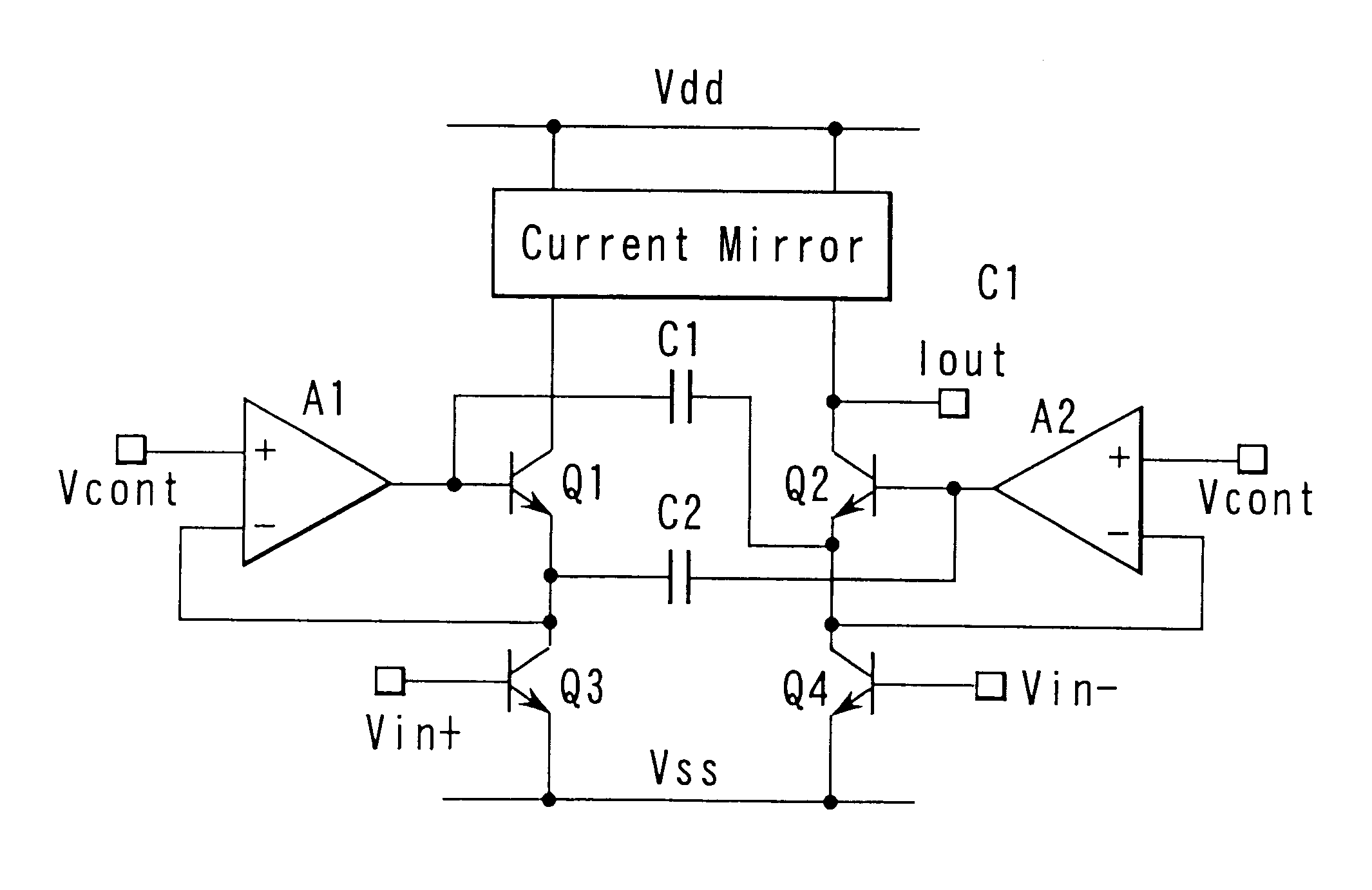
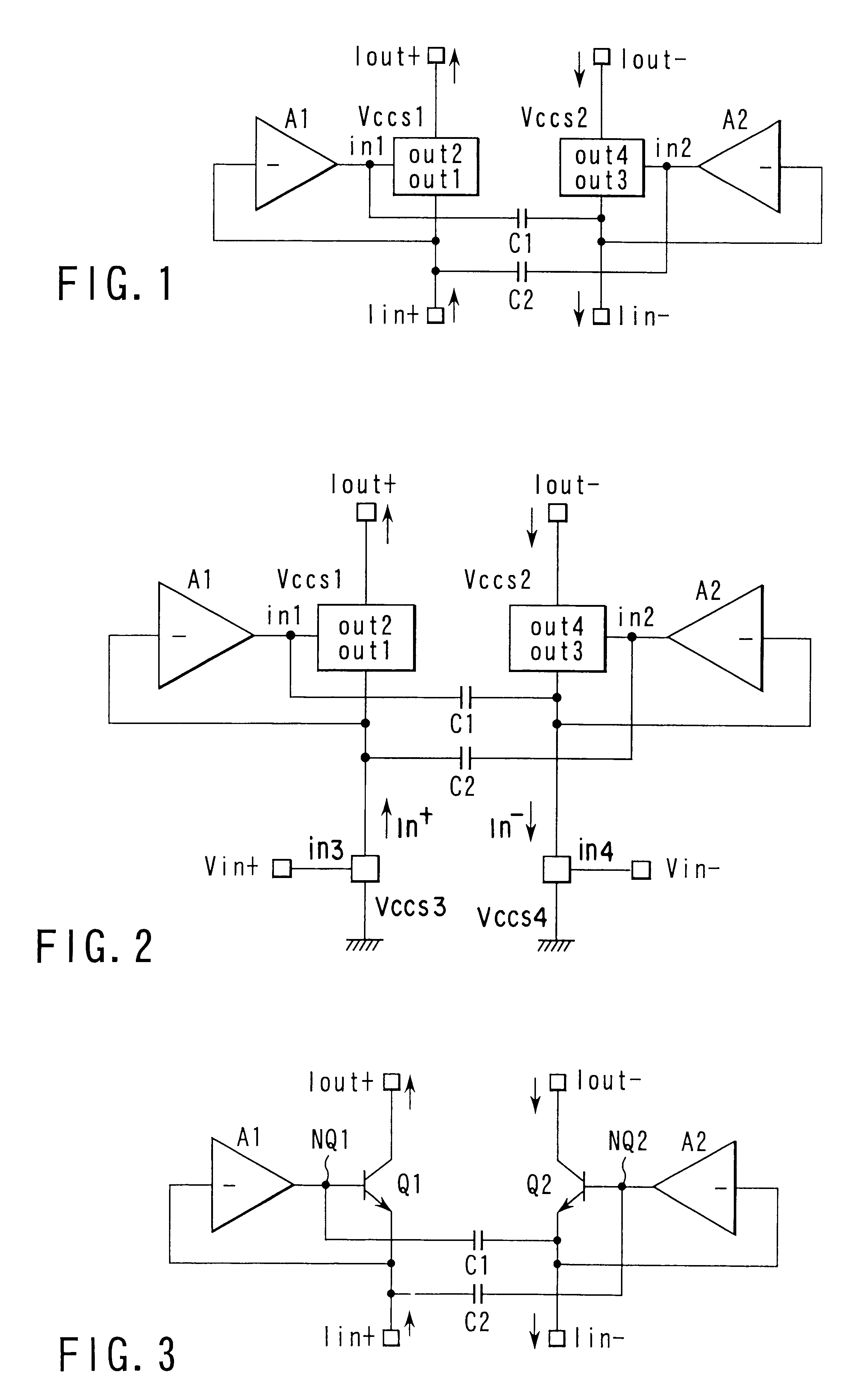
Examples
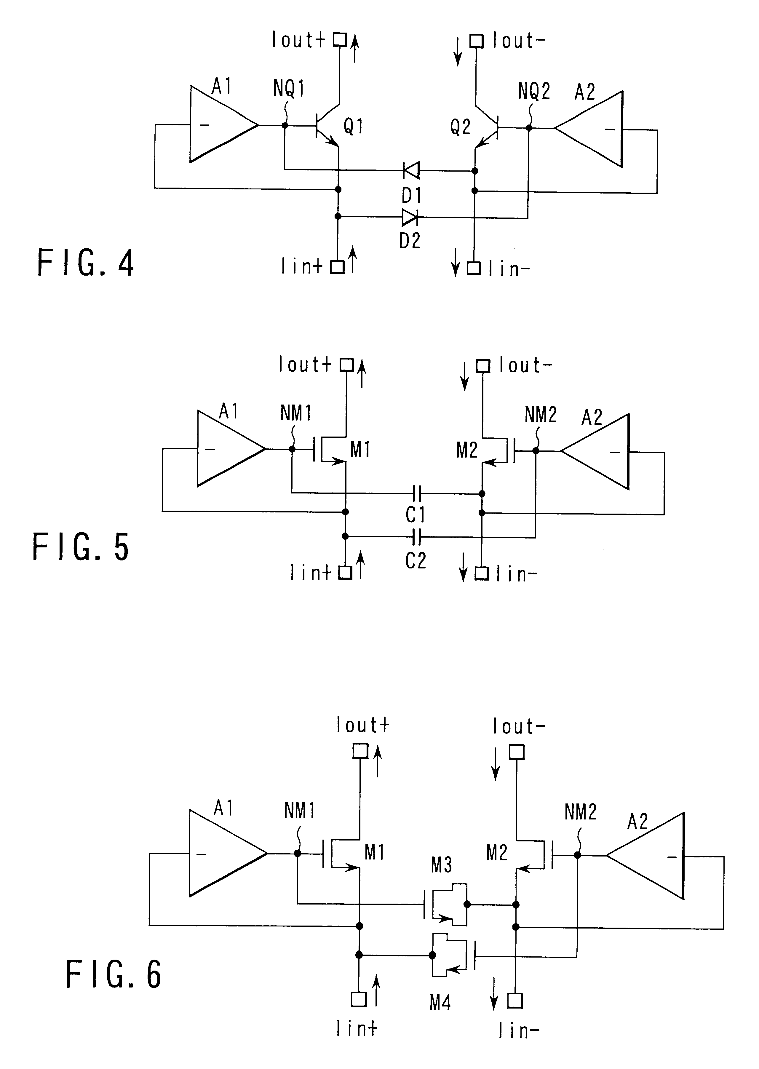
modification example 1-2
(Modification Example 1-2)
FIG. 4 is a circuit diagram of the impedance conversion circuit according to a modification example 1-2. In the example the capacity element (C1, C2) of the impedance conversion circuit shown in FIG. 3 is replaced with a pn junction diode (D1, D2). Even when the capacity of the pn junction diode is utilized instead of the capacity of MIM (Metal Insulator Metal) capacitor using a dielectric, the influence of the parasitic capacity can be reduced. Moreover, the diode is used in FIG. 4, but a diode-connected transistor similar to Q1, Q2 may be used. Furthermore, the capacity may be connected in parallel with D1, D2.
modification example 1-3
(Modification Example 1-3)
FIG. 5 is a circuit diagram of the impedance conversion circuit according to a modification example 1-3. The active element (Vccs1, Vccs2) of FIG. 1 is constituted of a metal insulator semiconductor field-effect transistor (MIS transistor). In the present modification example, a MOS transistor (MOSFET) was used as the MIS transistor. The capacitance of C1 and C2 are preferably set to be substantially equal to the parasitic capacity (mainly a capacity between gate and source) of a transistor M1, M2. Moreover, the MOS transistor (M1, M2) may be disposed in a silicon bulk substrate, or a silicon on insulator (SOI) substrate.
modification example 1-4
(Modification Example 1-4)
FIG. 6 is a circuit diagram of the impedance conversion circuit according to a modification example 1-4. In the present modification example the capacity element (C1, C2) of the impedance conversion circuit shown in FIG. 5 is replaced with the MIS transistor. Even when a drain and source of the MIS transistor having a structure similar to that of M1, M2 are short-circuited and the structure is used instead of (C1, C2), the influence of the gate parasitic capacity can be reduced. Additionally, in the aforementioned "similar structure", a material and thickness of a gate insulating film are substantially the same.
The capacity generated between a gate electrode of the MIS transistor (M3, M4) having a short-circuit between a drain electrode and a source electrode, and a reverse layer channel is about 1.5 times as large as the gate to source capacity operated with the same gate electrode area, under the voltage between the gate electrode and the source electrode...
PUM
 Abstract
Description
Claims
Application Information