Method and system for semiconductor wafer fabrication process real-time in-situ interactive supervision

a technology of real-time semiconductor wafers and fabrication processes, applied in semiconductor/solid-state device testing/measurement, instruments, photomechanical equipment, etc., can solve the problems of increasing the number of processing tools required to achieve the effect of achieving real-time status of semiconductor wafers after each processing step, avoiding unnecessary processing time and wafer waste, and speeding up wafer processing

Inactive Publication Date: 2002-03-26
IBM CORP
View PDF13 Cites 336 Cited by
  • Summary
  • Abstract
  • Description
  • Claims
  • Application Information

AI Technical Summary

Benefits of technology

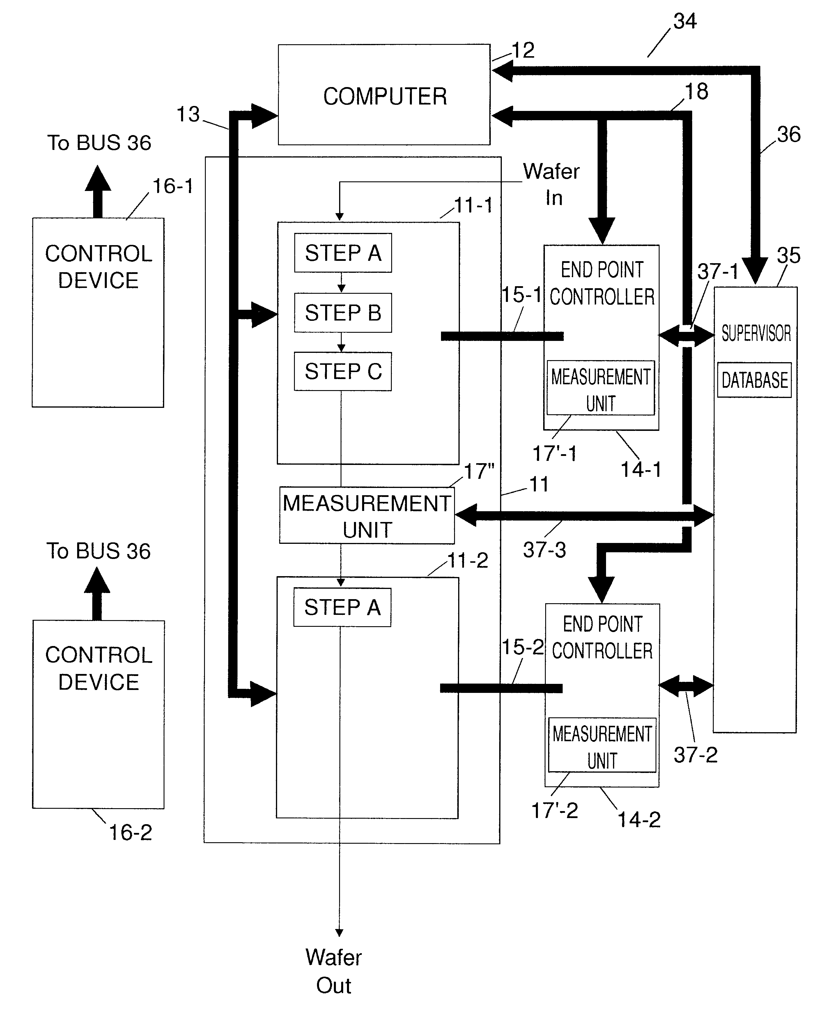
It is another object of the present invention to provide a method and a system for semiconductor wafer fabrication process real-time in-situ interactive supervision that get rid of misprocessing errors, process drifts and tool failures by real-time detection thereof during wafer processing.
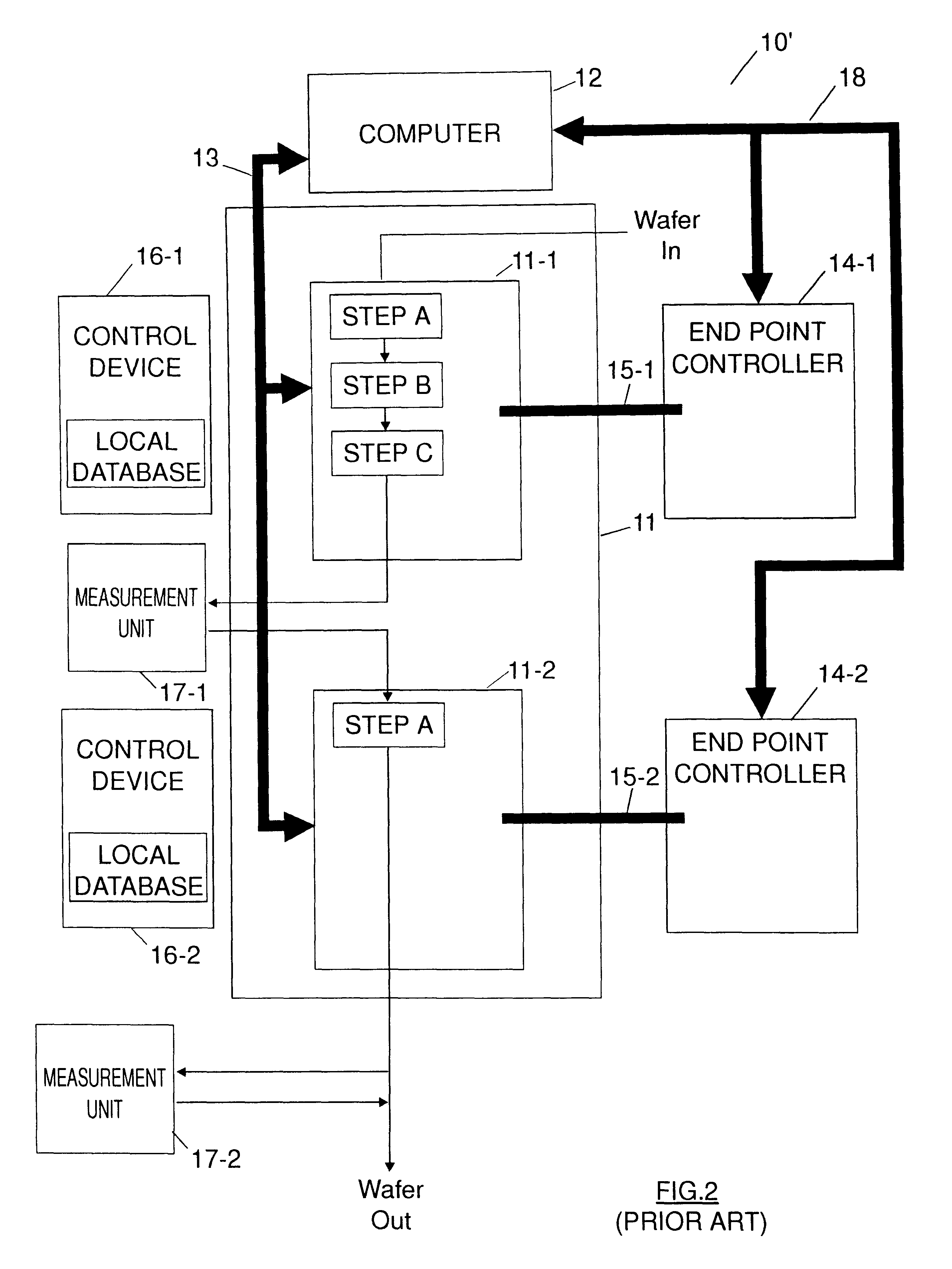
FIG. 2 shows an improved version, still conventional, of the FIG. 1 system which now includes different additional equipments (EPD controllers, control devices, . . . ) for a more efficient operation;

Problems solved by technology

For this reason, processing tools which are required to that end, are becoming more and more complex.
All these characterization techniques produce huge quantity of data of various types.
A stop generally occurs after a serious hardware failure such as a RF power shut-down or a gas flow missing.
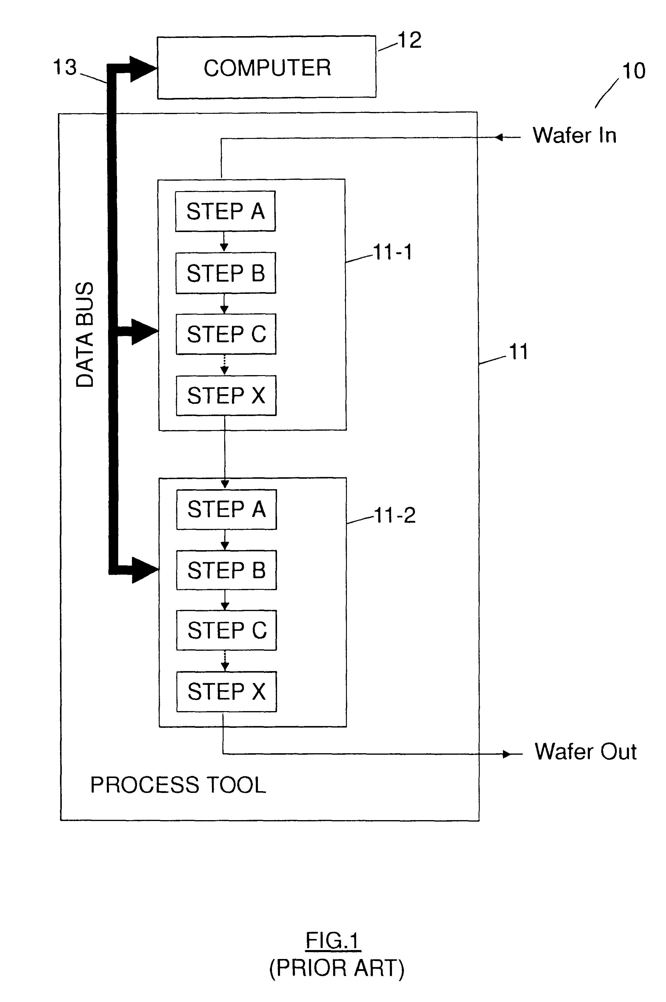
However, the real status of the wafer after each processing step is totally unknown for the computer.
In addition, using EPD controller 14-1 to control steps A and C does no guarantee a correct "AB ETCH" process.
Some serious problems that often occur at this stage of the fabrication process may lead to reject a number of wafers.
The wafer is definitely damaged and is no longer reworkable.
A deposition of polymers on the view-port surface of the AME 5000 plasma etcher will produce process drifts that could be detrimental to keep the wafer within specifications.
Finally, an electrical misfunction on the buses or a RF shut-down are typical examples of tool failures.
The operator must periodically adjust parameters in the course of the process depending on its evolution, making thereby very difficult any automation attempt.
Moreover, because there is no possibility to intervene during the process, a problem is only detected when a wafer is extracted from a chamber, so that it is too late to save the wafer which is often no longer reworkable.
Moreover, none of these systems is able to take profit of the wafer history (i.e. all the events that occurred to the wafer prior to the current step) to change a process parameter during the current step or in a subsequent step.
Moreover, these system configurations result in non automated tools because no clusterization is possible, so that the totality of the wafer processing cannot be performed in-situ in a multi-chamber tool.

Method used


Image

  • Method and system for semiconductor wafer fabrication process real-time in-situ interactive supervision
  • Method and system for semiconductor wafer fabrication process real-time in-situ interactive supervision
  • Method and system for semiconductor wafer fabrication process real-time in-situ interactive supervision

Examples


example i

As mentioned above, at the initial stage of the "AB ETCH" process, i.e. step A, photoresist layer AB1 is normally present. The case where structure 19 has no defect is represented by curves 26 to 29 in the graph of FIG. 4. As apparent from FIG. 4, the derivative signal S'1 (curve 27) exhibits a very sharp transient at the end of the step. Now turning to FIG. 8 which illustrates the signals 31, S'1, S2 and S'2 when the AB1 photoresist layer 24 is missing. In this case, the S'1 signal represented by curve 34 has a more gradual slope instead. This difference will be used by the expert information to distinguish the two cases. To characterize the absence of the AB1 photoresist layer, the following rule has been established: if signal S'1 is higher than 500 (arbitrary units) and lower than 1600 during at least about 25 s, the AB1 photoresist layer is considered missing. Then, the consequence of such a situation is considered for an appropriate response. If AB1 photoresist layer is missin...

example ii

Let us assume that the wafer has not been submitted to the AB1 lithography step. As a result, the two photoresist AB1 and AB2 layers 24 and 25 are present in their totality at the surface of the structure 19 before the wafer is processed at step A. FIG. 9 shows signals S1, S'1, S2 and S'2 in that particular situation. In this case, expert information provides selected signal S'2 of curve 35 which defines the etch rate and thus the etched thickness. The rule specifies that if etched thickness exceeds 10% of the nominal value, the process should be stopped, otherwise it will continue until the maximum allowed time be reached. Because, the etch end point of step A will never occur, the TEOS SiO2 layer 22 will never be etched, this is why the etch process must thus stop without delay. The alert code will be again "IMMEDIATE STEP STOP" and the recommended action is to by-pass steps B and C. In the instant case, the wafer is not damaged, it just needs to be reworked.

example iii

Still another frequent failure that occurs in the manufacturing at the "AB ETCH" level is the absence of the AB2 photoresist layer 25. If AB2 photoresist layer 25 is missing when step A is initiated in chamber 11-1, the chemistry that is currently used at this step, etches both the TEOS SiO2 material of layer 22 and the photoresist material of AB1 layer 24 at the same rate. In a few minutes, the totality of the AB1 photoresist is removed plus a large amount of the TEOS SiO2 material. As a consequence, the wafer needs to be rejected at this stage of the fabrication process. In this case, signal S'1 will be used, and as soon as an interference is detected, which means that TEOS SiO2 material is being etched, the etching is immediately stopped. FIG. 10 shows signals S1, S'1, S2 and S'2 in that particular situation, wherein signal S'1 is represented by curve 36. In this case, the rule is: starting from RATE TIME RT of signal S'1 for a maximum duration of 120 s, if signal S'1 amplitude r...


PUM

PropertyMeasurementUnit
thicknessaaaaaaaaaa
thickaaaaaaaaaa
wavelengthaaaaaaaaaa

Abstract

Method and system for real-time in-situ interactive supervision of a step performed in a tool during semiconductor wafer fabrication process. The system includes a tool and the computer attached thereto, an end point detection controller, a database and a supervisor to supervise the whole wafer processing for that step. The controller is used to monitor a key process parameter of the step and is adapted to perform in-situ measurements. The database contains the evolution of said process parameter in normal operating conditions and in all the identified deviations. It further contains the history of the wafer until this step and a reference to the batch and process names for this step and the wafer identification number. At the end of the step, the important process parameters and any alert code are stored in the database to up-date the wafer history. This technique allows a total clusterized wafer fabrication process and prevents wafer rejection.

Description

The present invention relates generally to the manufacture of semiconductor integrated circuits and more particularly to a method and a system for real-time in-situ interactive supervision of the semiconductor wafer fabrication process. In a dedicated tool controlled by a computer, a method is developed which includes the steps of monitoring in real-time in-situ a plurality of process parameters in parallel by an end-point controller. Analysis rules are developed to perform a comparison and associated rejection criteria are coded in the form of algorithms and likewise stored in a database. If a process deviation is detected, an alert code is flagged to signal an alarm and the adequate action is immediately taken and these data stored in the database may be used to up-date the operating conditions of a step before it takes place.Due to the constant integration density increase, the fabrication processes that are used to date in the manufacture of semiconductor wafers for the producti...

Claims


Application Information

Patent Timeline
Patent Type & Authority Patents(United States)
IPC IPC(8): G03F7/20H01L21/66H01L21/302H01L21/02H01L21/3065
CPCH01L22/20G03F7/70525
Inventor CORONEL, PHILIPPECANTELOUP, JEANMACCAGNAN, RENZOVASSILAKIS, JEAN-PHILLIPPE
Owner IBM CORP
Why Eureka
Try Eureka