

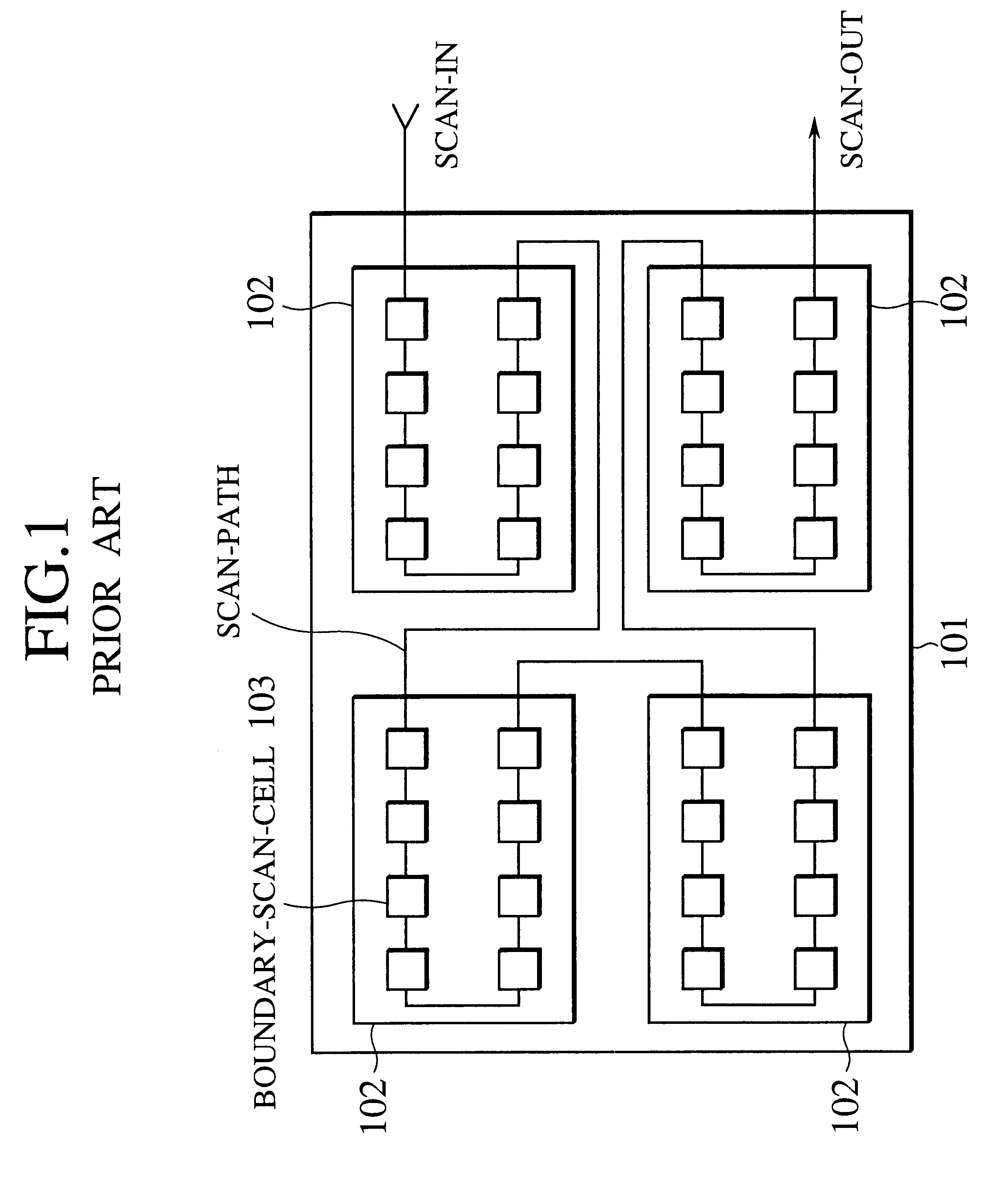
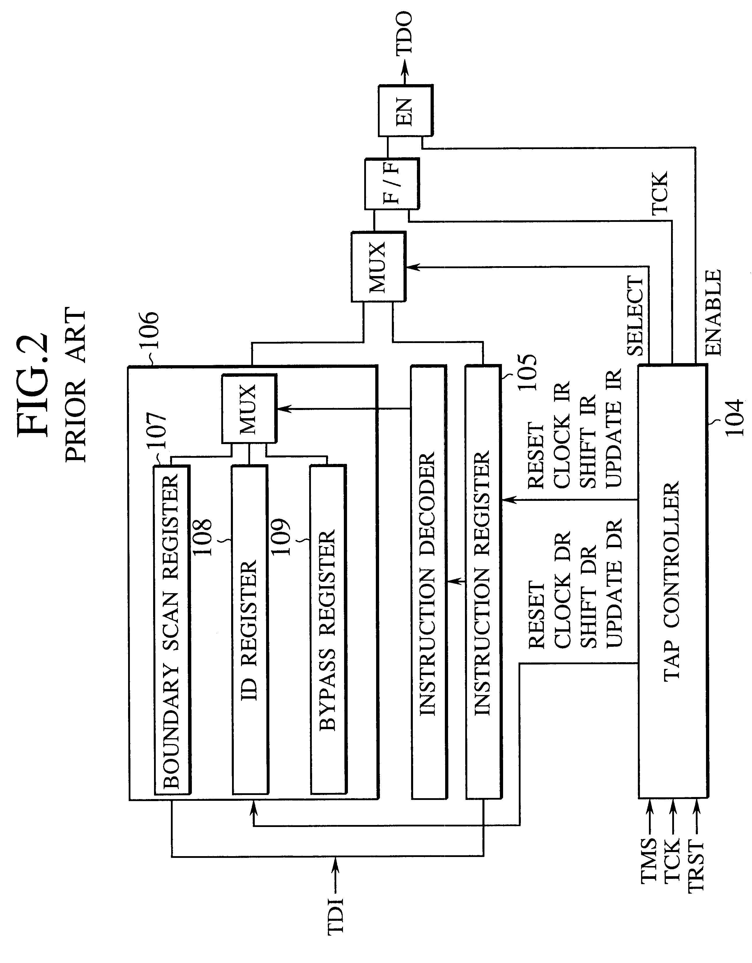
Semiconductor device provided with a boundary-scan test circuit
a test circuit and semiconductor technology, applied in the direction of electronic circuit testing, measurement devices, instruments, etc., can solve the problems of ineffective improvement of testability, large area penalty of test data register systems of this kind, and large area penalty
- Summary
- Abstract
- Description
- Claims
- Application Information
AI Technical Summary
Problems solved by technology
Method used
Image

Examples
first embodiment
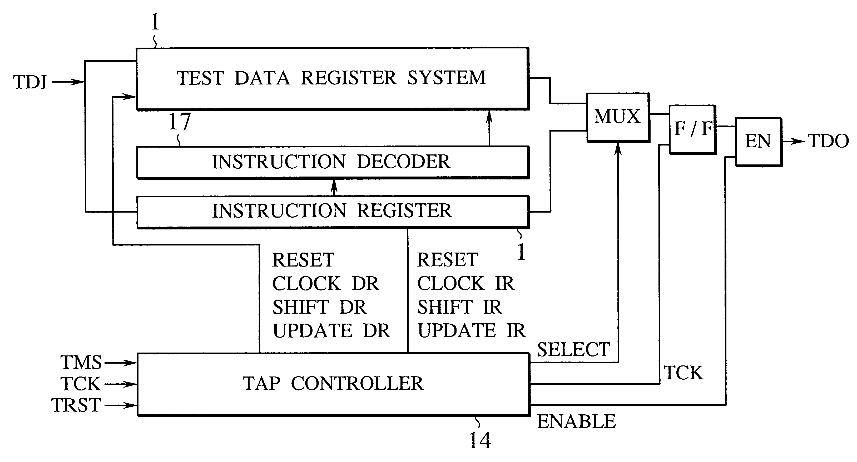
FIG. 8 is a block diagram of the Boundary-Scan test circuit in accordance with a In the figure, the Boundary-Scan test circuit is composed of a Test Access Port (TAP) controller 14, an instruction register 15 capable of serving as part of a scan path, an instruction decoder 17 for decoding an instruction as loaded onto the instruction register 15 and a test data register system 1 capable of serving as part of a scan path. The TAP controller 14 functions as a master controller for controlling the overall operation of the Boundary-Scan test circuit.
FIG. 9 is a block diagram showing the test data register system 1 of the Boundary-Scan test circuit in accordance with the first embodiment of the present invention.
In the figure, the test data register system 1 of the Boundary-Scan test circuit of this embodiment is mounted, for example, as part of the peripheral circuit of the semiconductor data storage device as illustrated in FIG. 10, which is a schematic diagram showing the layout of ...
second embodiment
FIG. 13 is a block diagram showing the test data register system 1 of the Boundary-Scan test circuit in accordance with the present invention.
In the figure, the Boundary-Scan register is composed of 32 stages of A circuits 4 for outputting the ID code and the extended data and a plurality of BS circuits 3 as 33rd and subsequent stages. These stages are connected in series. The Boundary-Scan register 2 is composed also of a multiplexer (MUX) 5 which selects and outputs one of the output signal of the last stage of the A circuits 4 and the output signal of the last stage of the BS circuit 3 in accordance with a BS / ID switching signal as generated from the instruction decoder.
FIG. 14 is a block diagram showing each of the A circuits 4 of this embodiment. In the figure, the A circuit 4 is composed of a multiplexer 18, a multiplexer 19 and a register 20. The multiplexer 18 serves to selectively output, in accordance with a register switching signal, one of data PI given through the pad 7...
third embodiment
FIG. 16 is a block diagram showing the test data register system 1 of the Boundary-Scan test circuit in accordance with the present invention. In the figure, the Boundary-Scan register 2 is composed of a plurality of BS circuits 3 connected in series. The initial stage BS circuit 3 functions also as a bypass register. The Boundary-Scan register 2 is composed also of a multiplexer 11 which selects and outputs one of the output signal of the initial BS circuits 3 and the output signal of the last stage of the BS circuit 3 in accordance with a BS / BP switching signal as generated from the instruction decoder.
Namely, the Boundary-Scan register 2 of this embodiment is provided also to function as the bypass register which has been separated provided in the case of the prior art technique. As a result, the area penalty resulting from the provision of the Boundary-Scan test circuit is alleviated.
PUM
 Abstract
Description
Claims
Application Information