Linearization bias circuit for BJT amplifiers

a bias circuit and amplifier technology, applied in amplifiers, amplifiers with semiconductor devices/discharge tubes, amplifier control details, etc., can solve problems such as limited output power, and achieve the effect of high impedan

Inactive Publication Date: 2002-07-30
INTELLECTUAL VENTURES I LLC
View PDF3 Cites 36 Cited by
  • Summary
  • Abstract
  • Description
  • Claims
  • Application Information

AI Technical Summary

Benefits of technology

The transconductance amplifier may be implemented as an emitter follower amplifier with an isolation resistor. The output of the transconductance amplifier may have a high impedance at a fundamental frequency of the RF signal, so that it is able to control the DC bias point without affecting the RF signal.

Problems solved by technology

The output component results from the output power being limited, depending upon the load, either by voltage swing clipping or by the load current exceeding the DC collector current.

Method used


Image

  • Linearization bias circuit for BJT amplifiers
  • Linearization bias circuit for BJT amplifiers
  • Linearization bias circuit for BJT amplifiers

Examples


Embodiment Construction

Since control circuits generally process DC, it is desired to find a relationship between the DC current scale factor I.sub.0 (x) and the transconductance scale factor 2I.sub.1 (x) / x. One such approximation is linear regression according to the following equation 8: ##EQU6##

which indicates that constant gain may be achieved with a bias control circuit for the amplifier BJT that implements an approximation according to the following equation 9: ##EQU7##

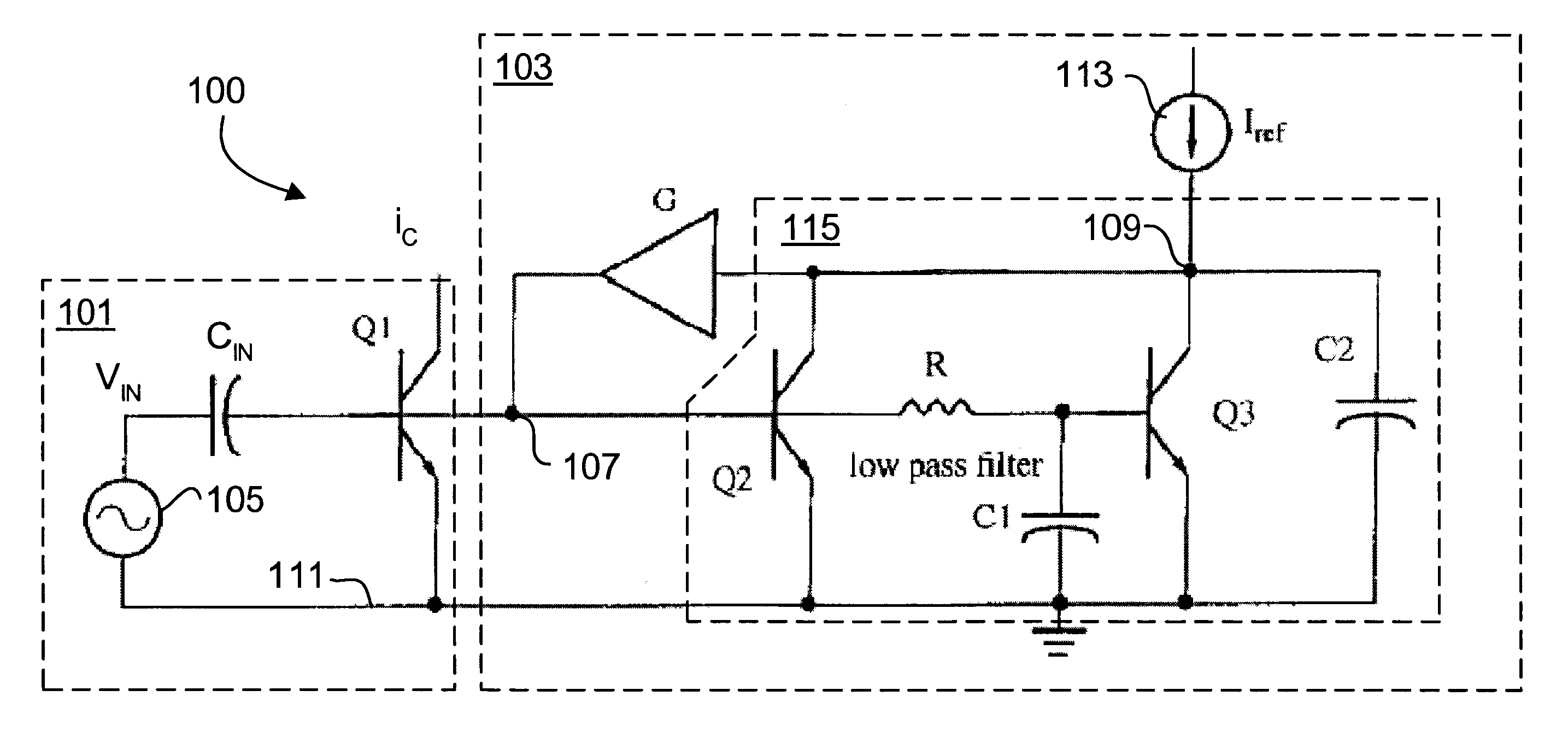
FIG. 1 is a schematic diagram of an RF BJT amplifier circuit 100 according to an embodiment of the present invention. The RF BJT amplifier circuit 100 includes a BJT amplifier circuit 101, with primary BJT amplifier Q1, coupled to a linearization bias circuit 103. As described below, the linearization bias circuit 103 incorporates the relationships described in equations 8 and 9 in order to maintain the transconductance of the BJT Q1 substantially constant in the presence of varying input voltage amplitudes of an input radio frequency ...


PUM


Abstract

A linearization bias circuit for an RF BJT amplifier including a reference circuit, a current device and a transconductance amplifier. The linearization bias circuit controls the operating point of the BJT amplifier based on signal level of an input RF signal. The current device provides a constant reference current to the reference circuit, where the constant reference current has a level that is based on a desired collector current of the BJT amplifier. The reference circuit applies a predetermined relationship between DC and AC scale factors of collector current of the BJT amplifier. The transconductance amplifier asserts its output to maintain the constant reference current into the reference terminal of the reference circuit, and in doing so controls the base terminal of the BJT amplifier to modify its operating point to substantially maintain constant transconductance in the presence of varying input voltage amplitudes of the input RF signal.

Description

The present invention relates to bipolar junction transistor (BJT) amplifiers, and more particularly to linearization bias circuit for BJT amplifiers that extends the compression point by keeping transconductance constant in the presence of varying input voltage amplitudes of an input radio frequency (RF) signal.DESCRIPTION OF RELATED ARTThe 1 decibel (dB) compression point for a radio frequency (RF) bipolar junction transistor (BJT) amplifier has both an input and an output component. The output component results from the output power being limited, depending upon the load, either by voltage swing clipping or by the load current exceeding the DC collector current. The output limited compression point should be reasonably sharp. The input component of compression results from the exponential relationship between base-emitter voltage and collector current. As the peak of the AC component of the base-emitter voltage approaches the thermal voltage V.sub.T, the transconductance and inpu...

Claims


Application Information

Patent Timeline
Patent Type & Authority Patents(United States)
IPC IPC(8): H03G1/00H03F1/32
CPCH03F1/30H03F1/32H03G1/0035H03F2200/453H03F2200/456
Inventor PRENTICE, JOHN S.
Owner INTELLECTUAL VENTURES I LLC
Why Eureka
Try Eureka