
Eureka
For R&D, Eureka makes reading and utilizing patents & technical documents easy.
Eureka AIR
Designed for self-driven R&D workflows. Generate viable solutions, solve complex R&D challenges, empower your innovation with AI.

Eureka Materials
Designed for material experts only. Revolutionize your material R&D, from search, analyze, to developing new materials.

TechResearch
Generate reliable direction feasibility study reports for your R&D in just a few steps.

TechSeek
Discover and master advanced knowledge NOW. Basics, ideas, possibilities, all at once.

TechMind
As an expert in R&D Theories, TechMind can generates customized viable solutions instantly.

TechRisk
Analyze your overall solution with one click, know your potential R&D risks in advance.

TechMonitor
Get weekly tech updates, stay abreast of the latest tech innovations and key insights.
Integrated semiconductor device with wafer-level burn-in circuit and function decision method of wafer-level burn-in circuit
- Summary
- Abstract
- Description
- Claims
- Application Information
AI Technical Summary
Problems solved by technology
Method used
Image


Examples
embodiment 1
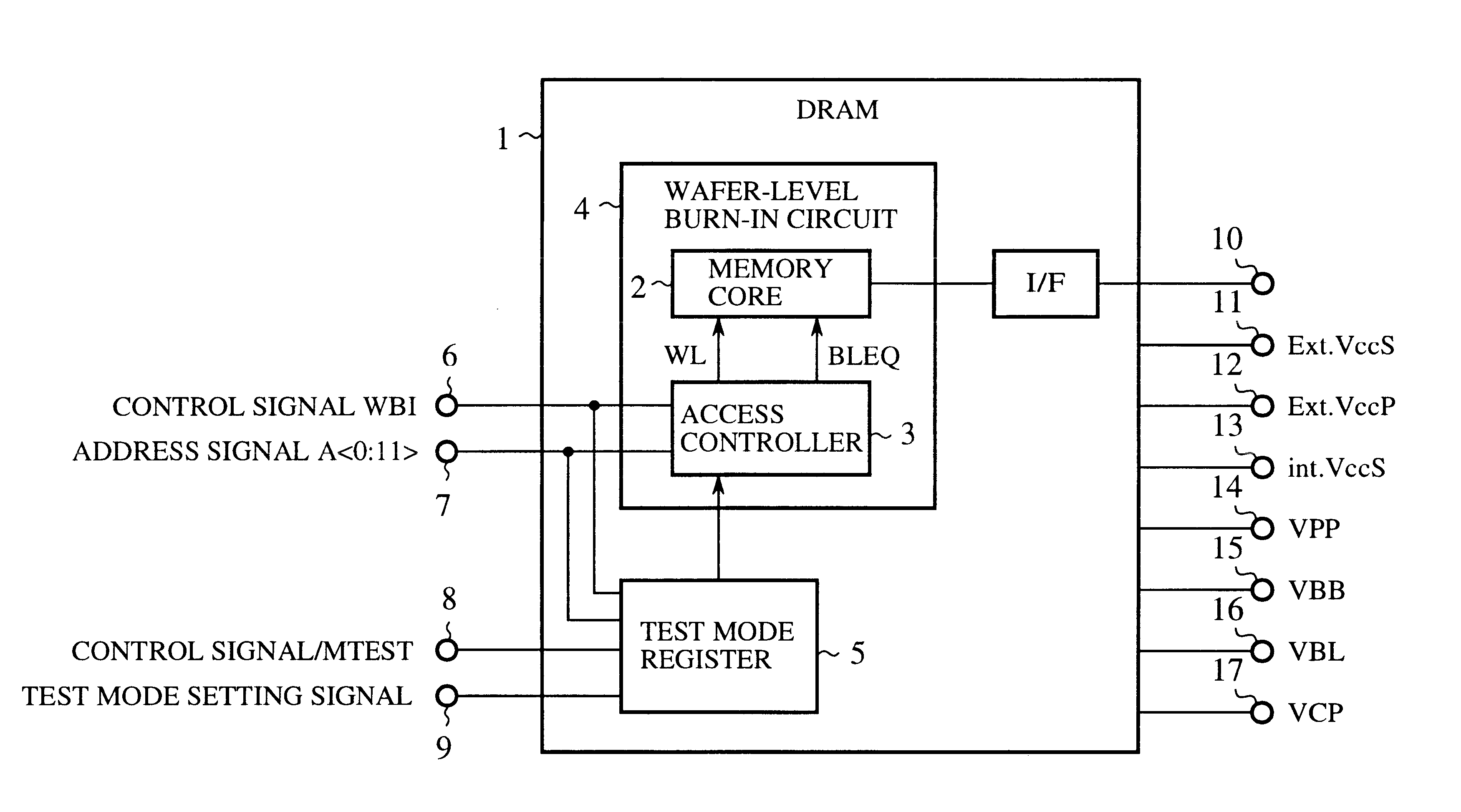
FIG. 1 is a block diagram showing a configuration of an integrated semiconductor device with a wafer-level burn-in circuit in accordance with the present invention. In FIG. 1, the reference numeral 1 designates an integrated semiconductor device such as a DRAM and / or SRAM, which can also include various types of logic circuits besides the DRAM and / or SRAM. In FIG. 1, however, the logic circuits are omitted for the sake of simplicity.
The reference numeral 2 designates a memory core including a plurality of memory cells; 3 designates an access controller for controlling wafer-level burn-in operation; 4 designates a wafer-level burn-in circuit consisting of the memory core 2 and access controller 3; 5 designates a test mode register; and 6 designates a pin for inputting a control signal WBI for setting the access controller 3 in a wafer-level burn-in (WLBI) mode.
The reference numeral 7 designates pins for supplying the integrated semiconductor device 1 with an address signal A, the val...
embodiment 2
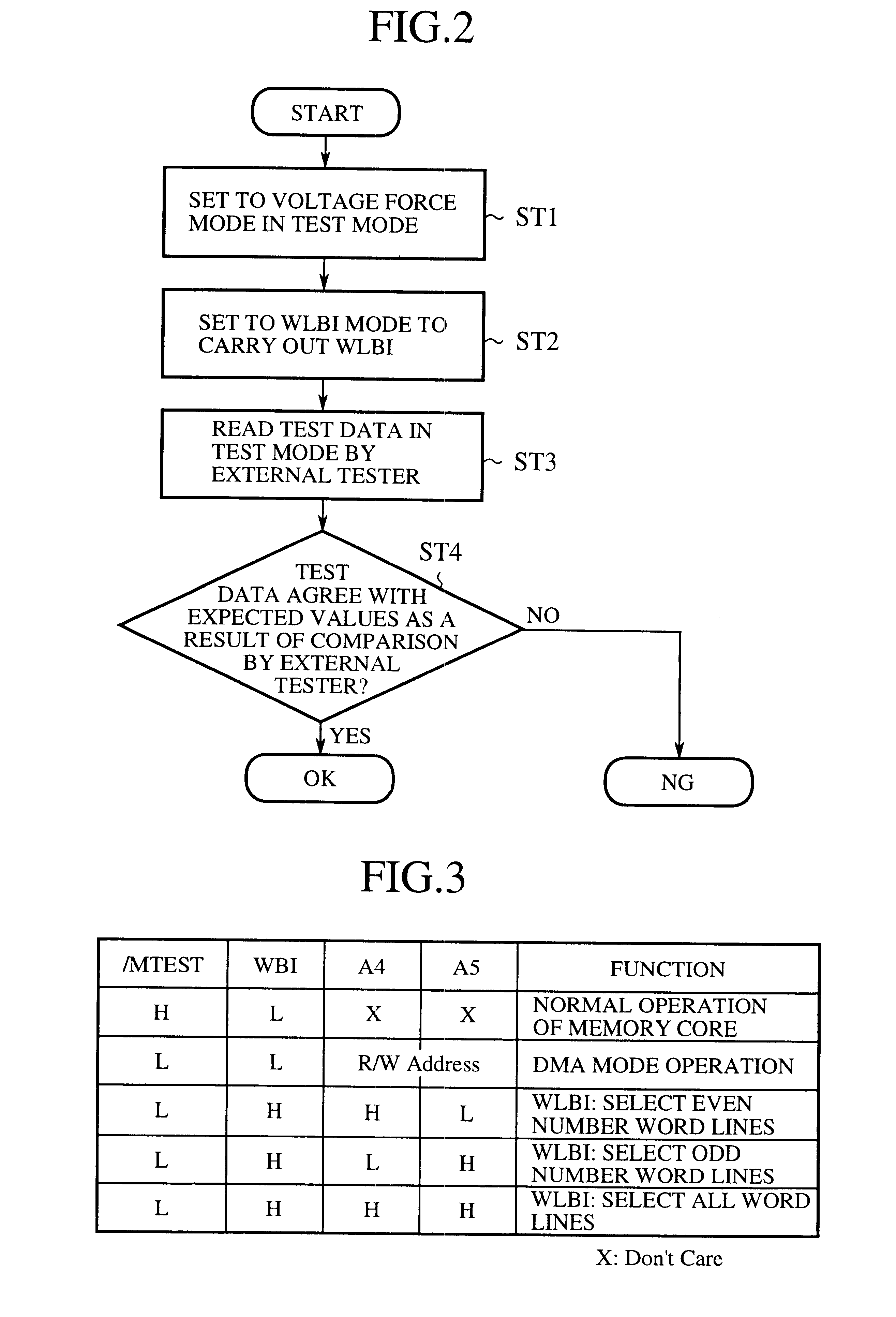
FIG. 8 is a block diagram showing a configuration of an embodiment 2 of the integrated semiconductor device with wafer-level burn-in circuit in accordance with the present invention. In FIG. 8, the reference numeral 18 designates an integrated semiconductor device. The reference numeral 19 designates an expected value comparator for comparing the data read from the memory core 2 with the expected values, and supplying the compared result to the external device (not shown) outside the integrated semiconductor device 18 through a pin 20 as the decision result of the wafer-level burn-in.
Since the remaining components are the same as those of the foregoing embodiment 1, they are designated by the same reference numerals and the description thereof is omitted here. Although the integrated semiconductor device 18 with the wafer-level burn-in circuit 4 as shown in FIG. 8 consists of a DRAM, it can be a mixture of the DRAM and / or SRAM together with various types of logic circuits. However, ...
PUM
 Abstract
Description
Claims
Application Information
 - R&D Engineer
- R&D Manager
- IP Professional
- Industry Leading Data Capabilities
- Powerful AI technology
- Patent DNA Extraction
Browse by: Latest US Patents, China's latest patents, Technical Efficacy Thesaurus, Application Domain, Technology Topic, Popular Technical Reports.
© 2024 PatSnap. All rights reserved.Legal|Privacy policy|Modern Slavery Act Transparency Statement|Sitemap|About US| Contact US: help@patsnap.com