Logic circuit with single charge pulling out transistor and semiconductor integrated circuit using the same

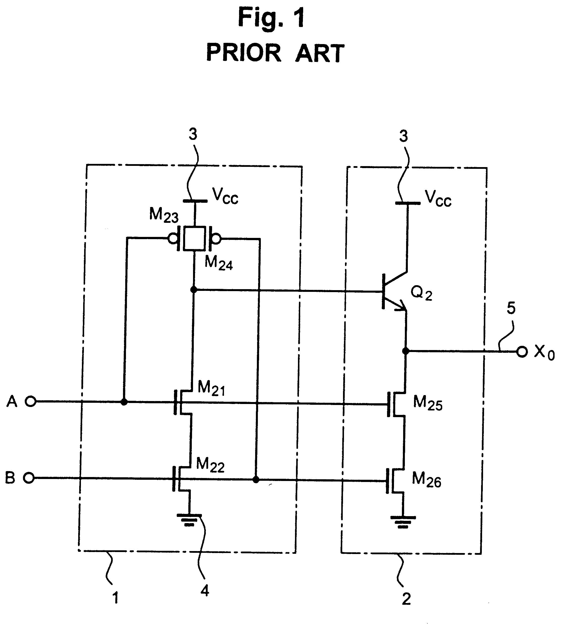
a logic circuit and integrated circuit technology, applied in logic circuits, digital storage, pulse techniques, etc., can solve the problems of delay in the operation of a preceding logic circuit stage and serious impedemen

Inactive Publication Date: 2002-09-03
RENESAS ELECTRONICS CORP
View PDF4 Cites 15 Cited by
  • Summary
  • Abstract
  • Description
  • Claims
  • Application Information

AI Technical Summary

Problems solved by technology

However, by increasing the gate width, the input capacitance viewed from the input signal is increased resulting in a delay in the operation of a preceding logic circuit stage (not shown).
Where a plurality of logic gate stages are present, it is necessary for the high speed operation of the circuit to improve the fan-out characteristic, i.e., the relation between the ratio of the input capacitance to the output load capacitance and the delay time, but this has been seriously impeded by the capacity reduction of the series n-channel MOS transistors M.sub.21, M.sub.22, M.sub.25 and M.sub.25.

Method used


Image

  • Logic circuit with single charge pulling out transistor and semiconductor integrated circuit using the same
  • Logic circuit with single charge pulling out transistor and semiconductor integrated circuit using the same
  • Logic circuit with single charge pulling out transistor and semiconductor integrated circuit using the same

Examples


first embodiment

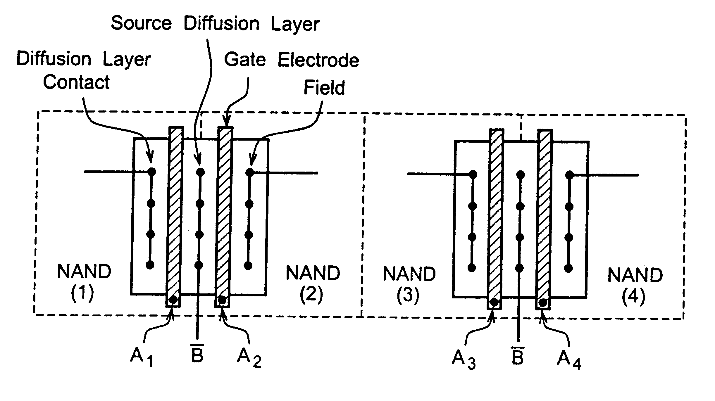
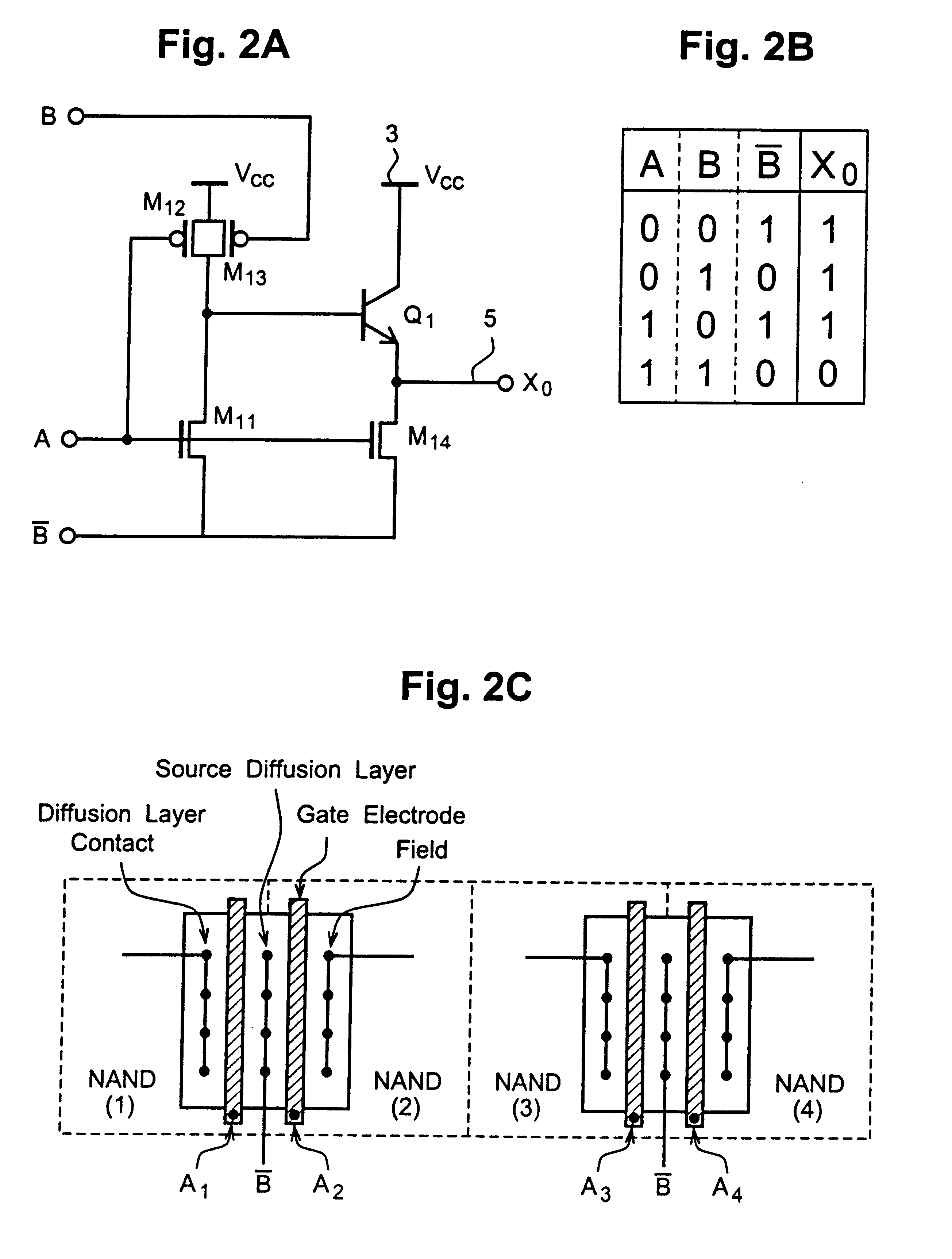
FIG. 2A is a circuit diagram showing the logic circuit according to the invention applied to a two-input NAND logic circuit having the BiCMOS structure. Comparing FIGS. 2A and 1, this embodiment of the invention is significantly different from the prior art NAND circuit in that the current paths for pulling down output stage BiP transistor base potential and pulling out charge from the load are constituted by independent n-channel MOS transistors M.sub.11 and M.sub.14, respectively, instead of the series n-channel MOS transistors M.sub.21 and M.sub.22 and the series n-channel MOS transistors M.sub.25 and M.sub.26 in the prior art.

In this embodiment, an input signal A is inputted to the gate of a p-channel MOS transistor M.sub.12 as well as the gate of the n-channel MOS transistor M.sub.11. The source of the p-channel MOS transistor M.sub.12 is connected to a high potential power supply line 3 (at V.sub.cc). A separate input signal B is inputted to the gate of a p-channel MOS transis...

second embodiment

the invention will now be described with reference to FIG. 3. In this embodiment, only a single p-channel MOS transistor M.sub.32 is used for the pull-up of the base potential on an output stage BiP transistor Q.sub.3. The p-channel MOS transistor M.sub.32 is normally held "on" with its gate held at the ground potential from a ground line 4. The input signals are thus only the signal A and the inverse signal and, unlike in the preceding first embodiment, the inverse signal .gradient.B is unnecessary. This embodiment also has a lesser number of elements than that in the first embodiment by one.

In this embodiment, in the other cases than when the signal A and the inverse signal .gradient.B come up with "high" and "low", respectively, p-channel MOS transistors M.sub.31 and M.sub.32 are "off". Thus, the BiP transistor Q.sub.3 is held "on" with its base potential held pulled up to the supply voltage V.sub.cc by the p-channel MOS transistor M.sub.32. As a consequence, the Bip transistor Q...

third embodiment

the invention will now be described with reference to FIG. 4. Referring to the figure, this embodiment is the same as the preceding embodiments in the point wherein the output X.sub.0 is pulled down by using a single n-channel MOS transistor M.sub.41. A feature of this embodiments resides in that the output X.sub.0 is pulled up by using only BiP transistors. The inverse signal .gradient.B which is inputted to the source of the n-channel MOS transistor M.sub.41, is also inputted to the base of the BiP transistor Q.sub.41, and the inverse signal .gradient.A inverse to the signal A is inputted to a base of a BiP transistor Q.sub.42 which is parallel with the transistor Q.sub.41.

In this embodiment, when the signal A and the inverse signal .gradient.B become "high" and "low", respectively (i.e., A=1, B=1), the n-channel MOS transistor M.sub.41 is turned on. At this time, the inverse signals .gradient.A and .gradient.B both become "low", and the two BiP transistors Q.sub.41 and Q.sub.42 a...


PUM


Abstract

A logic circuit performs a predetermined logic operation by supplying charge to an external load or pulling out charge therefrom according to a combination of the states of a plurality of externally inputted binary signals. The logic circuit includes a first transistor for supplying charge through an output terminal to the external load and a second transistor for pulling out the charge from the load through the output terminal. One of the first and second transistors is constituted by a MOS field-effect transistor having a drain connected to the output terminal. The MOS field-effect transistor has a source receiving an inverse signal inverse to a signal combined for logic operation with an input signal inputted to a gate of the MOS field-effect transistor. The number of the series transistors is reduced, resulting in an increase of the current capacity and in a reduction of the layout area. Adjacent ones of the logic circuits have a common source diffusion layer so that the load capacitance with respect to the inverse signal can be significantly reduced, thus enabling the high speed operation.

Description

(1) Field of the InventionThe present invention relates to logic circuits and semiconductor integrated circuits using the same, and more particularly to logic circuits which can be advantageously utilized in multiple input circuits, such as semiconductor memory decoder circuits, provided in an array form, and semiconductor integrated circuits using theame.(2) Description of the Related ArtAs an example of the prior art multiple input logic circuit, a two-input NAND circuit comprising a bipolar transistor and a MOS transistor (this structure being hereinafter referred to as BiCMOS structure) will now be described. FIG. 1 is circuit diagram showing the NAND circuit. As shown, the NAND circuit comprises a logic circuit stage 1 having a CMOS transistor structure and an output stage 2 having bipolar / MOS transistor 710 structure. Specifically, the logic circuit stage 1 includes a parallel circuit of two p-channel MOS transistors M.sub.23 and M.sub.24 and a series circuit of two n-channel ...

Claims


Application Information

Patent Timeline
Patent Type & Authority Patents(United States)
IPC IPC(8): H03K19/0944G11C11/40G11C11/408G11C11/413H03K19/017H03K19/08H03K19/20
CPCH03K19/09448G11C11/40
Inventor TAKAHASHI, HIROYUKISATO, MITSURU
Owner RENESAS ELECTRONICS CORP
Why Eureka
Try Eureka