Optoelectronic interconnect module

a technology of optoelectronic interconnection and module, applied in the field of optoelectronic interconnect modules, can solve the problems of increasing production costs, causing electromagnetic interference with surrounding equipment, and prone to generate undesired emissions of electronic components and circuits within the modules, so as to reduce production costs, prevent unintentional radiation, and minimize signal distortion

Inactive Publication Date: 2002-09-24
STRATOS INT
View PDF14 Cites 75 Cited by
  • Summary
  • Abstract
  • Description
  • Claims
  • Application Information

AI Technical Summary

Benefits of technology

A consequence of the objective of the present invention is to minimize signal distortion.
Another consequence of the objective of the present invention is to prevent unintentional radiation.
A further consequence of the objective of the present invention is to reduce production costs.

Problems solved by technology

At these high data rates, electronic components and circuitry within the module are prone to generate undesired emissions and create electromagnetic interference with the surrounding equipment.
Furthermore, the bend 72 in the connecting wires 62 increases production costs and decreases reliability of the optoelectronic interconnect module 50.
The bend in connecting wires, which is basic to the electrical interconnection of both the referenced prior arts embodiments shown in FIGS. 1 and 2, poses basic limitations for ultra-fast optoelectronic transceiver performance.
increases production cost
decreases reliability
As the interconnect impedance (Z) deviates from the system impedance (Z), frequency-dependent signal reflections will occur at the impedance mismatch, causing signal distortion.

Method used


Image

  • Optoelectronic interconnect module
  • Optoelectronic interconnect module
  • Optoelectronic interconnect module

Examples


Embodiment Construction

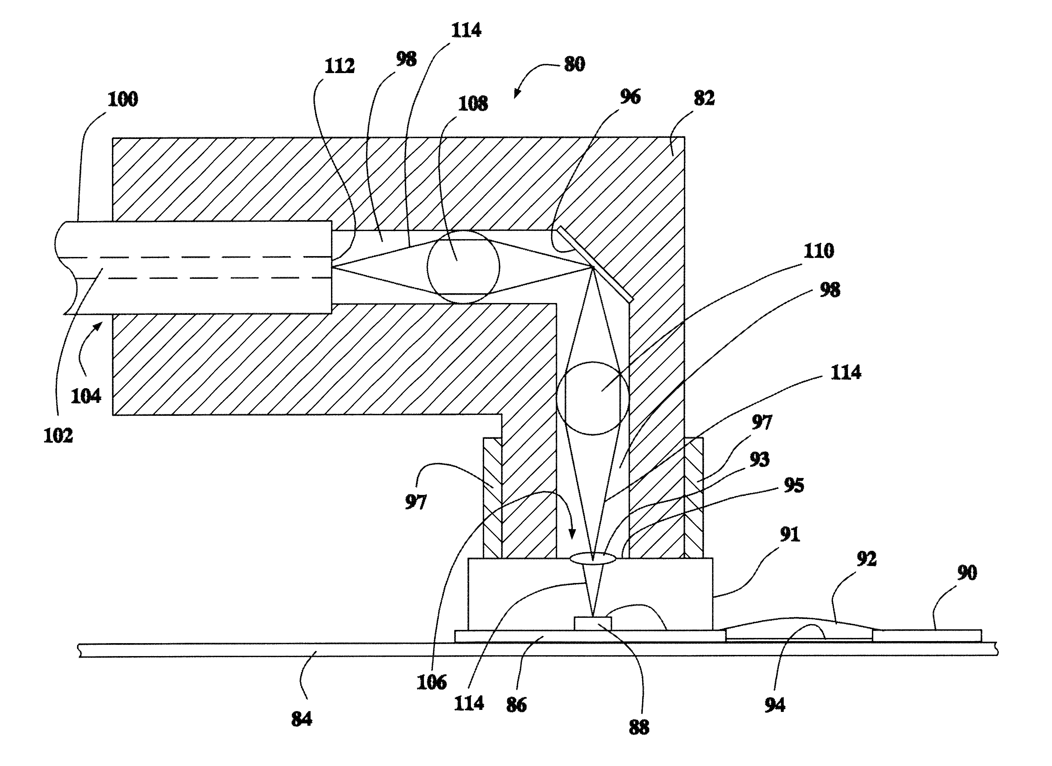
With reference to FIG. 4, the preferred embodiment of the optoelectronic interconnect module in accordance with the present invention is presented. The optoelectronic interconnect module 80 includes a housing 82 mounted to a circuit substrate or printed circuit board 84. The printed circuit board 84 is preferably constructed of a ceramic material. The housing 82 is preferably constructed of a polymer, such as plastic, but may also be constructed of glass, ceramic, or a micro-machined semiconductor. A base 86 for supporting a semiconductor die 88 is mounted to the circuit board 84.

The die 88 is hermetically sealed within a metal cover 91. A transparent window 93 is located on the top 95 of the metal cover 91 and opposite the die 88. The transparent window 93 enables optical radiation 114 to pass in or out of the hermetically sealed metal cover 91. In a receiver, the die 88 receives optical radiation 114 through the transparent window 93. In a transmitter, the die 88 emits optical rad...


PUM


Abstract

An optoelectronic interconnect module comprising a housing having a first aperture on a first side of the housing for receiving an optical ferrule and a second aperture on a second side of the housing for receiving a semiconductor die. A mirror is mounted within the housing at an angle for reflecting optical transmissions between the first and second apertures. A first optical lens is mounted between the first aperture and the mirror, and a second optical lens is mounted between the second aperture and the mirror. The optoelectronic interconnect module transmits an electronically modulated optical signal between an optical fiber in the first aperture and an optoelectronic semiconductor die adjacent to the second aperture within a mutually orthogonal plane.

Description

The present invention relates generally to optoelectronic interconnect modules for fiber optic communications. The present invention relates more specifically to an optoelectronic interconnect module enabling an optical transmitting or receiving semiconductor die to be mounted to a substrate with an optical axis perpendicular to an optical ferrule mounted to the optoelectronic interconnect module.Ultrafast optoelectronic transmitters are utilized in data communications systems wherein optical beams are modulated with electronic binary data pulses. The electronic pulses are conveyed by means of metallic conductors to a light-emitting semiconductor device, the modulated output of which may be transmitted over optical media (i.e., fiber optic cables).Optoelectronic interconnect modules or optical subassemblies may be configured for direct mounting to a circuit substrate or a printed circuit board within the host system. In this arrangement, contact pins extend from the module and are t...

Claims


Application Information

Patent Timeline
Patent Type & Authority Patents(United States)
IPC IPC(8): G02B6/42
CPCG02B6/4214
Inventor DWARKIN, ROBERTRAPALA, GREGG
Owner STRATOS INT
Why Eureka
Try Eureka