

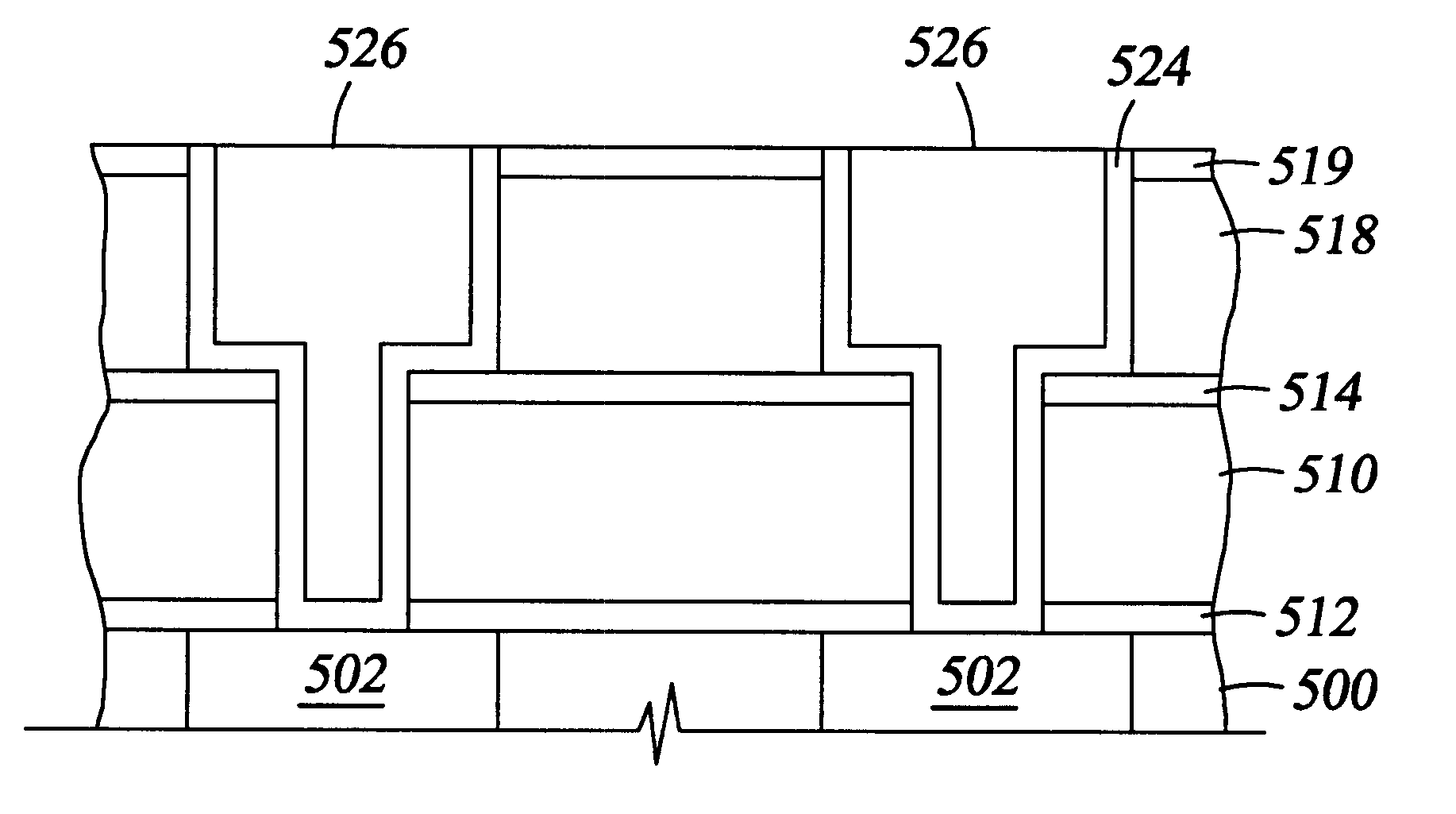
CVD plasma assisted lower dielectric constant sicoh film
a dielectric constant and film technology, applied in chemical vapor deposition coatings, transportation and packaging, coatings, etc., can solve the problem of difficult control of partially fragmented cyclic precursors
- Summary
- Abstract
- Description
- Claims
- Application Information
AI Technical Summary
Problems solved by technology
Method used
Image

Examples
example 1
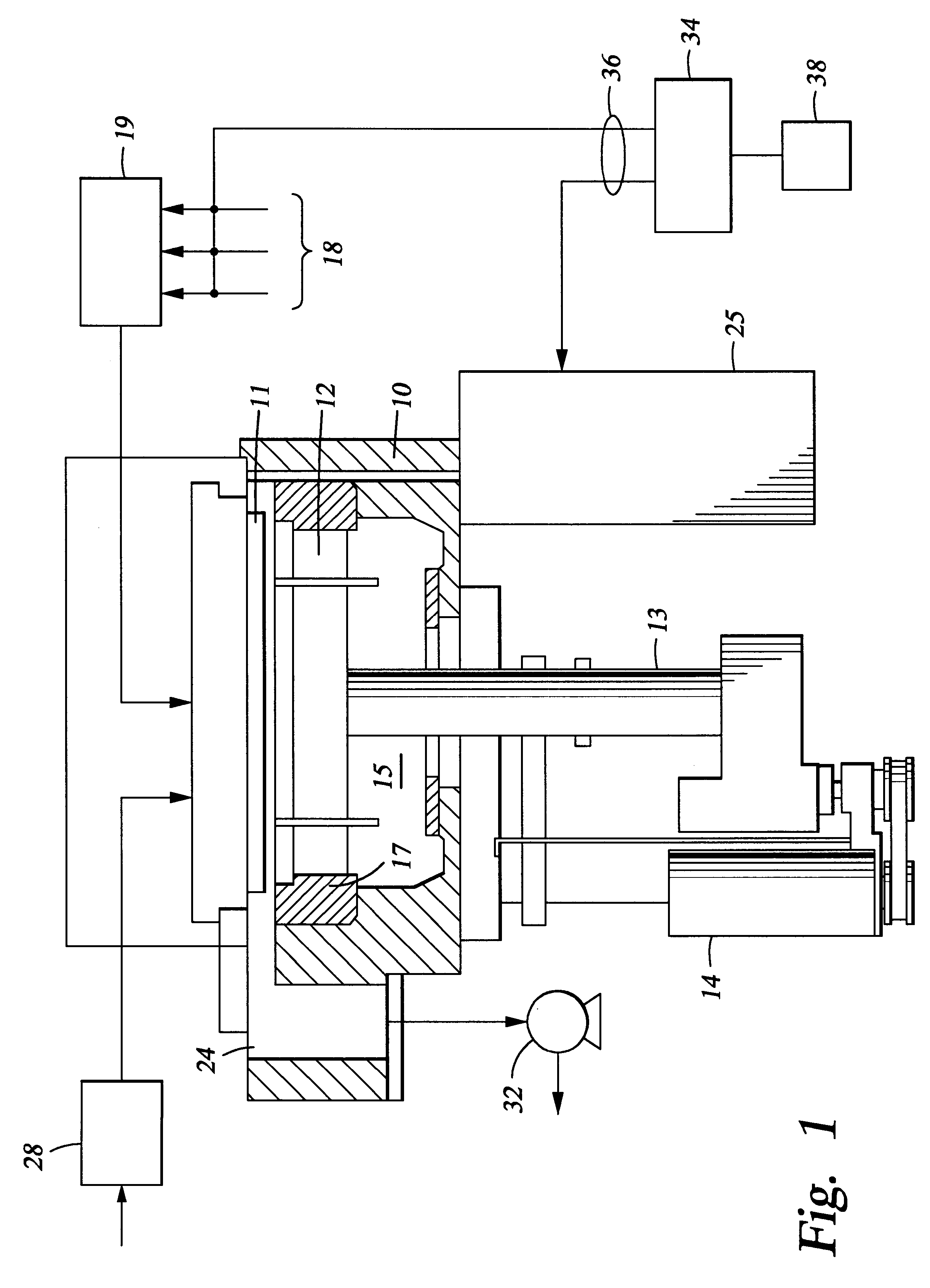
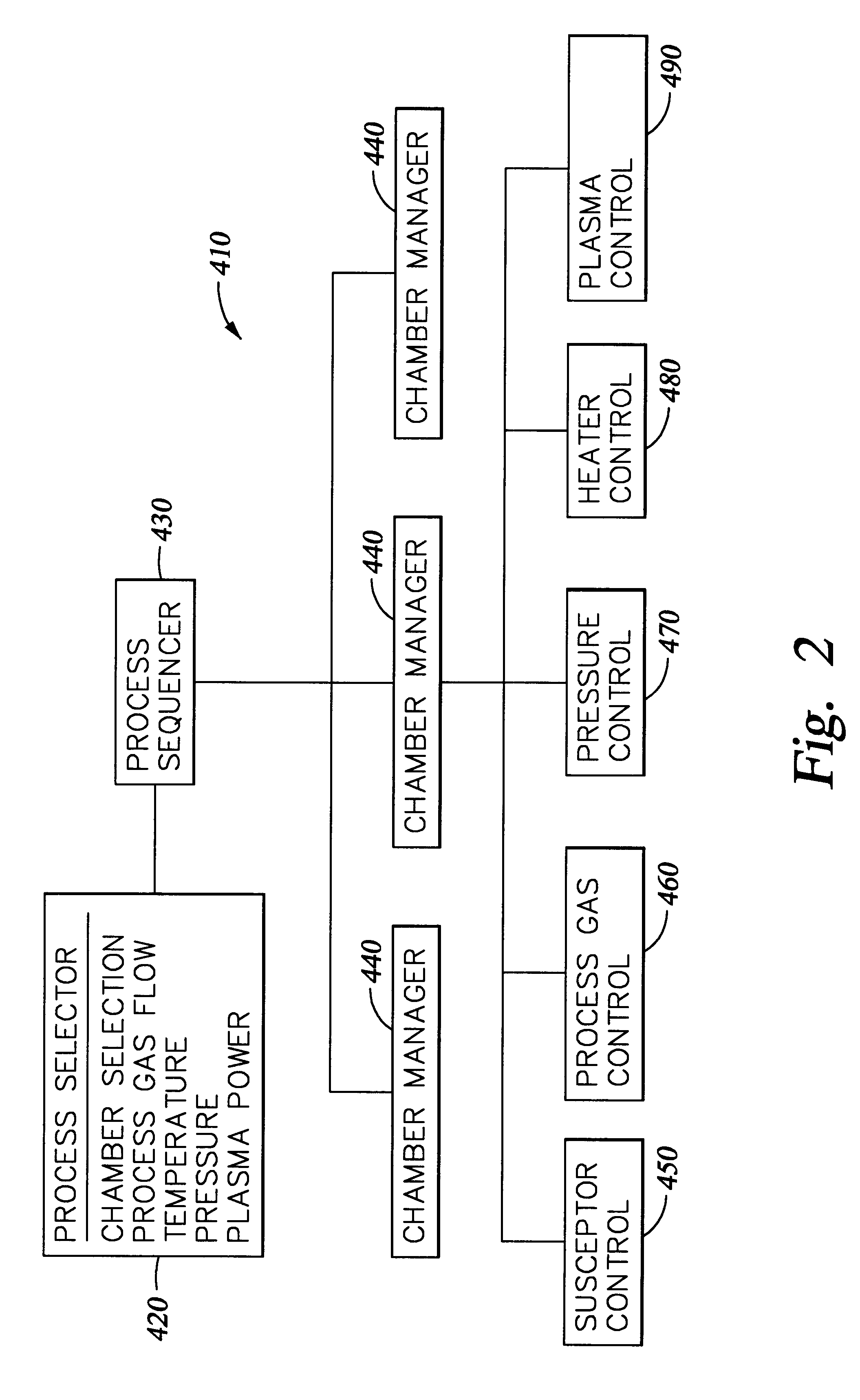
A low dielectric constant film was deposited on a substrate from the following reactive gases at a chamber pressure of 9 Torr and temperature of 350.degree. C.
Octamethylcyclotetrasiloxane (OMCTS), at 136 sccm (1800 mg / min);
Trimethylsilane (TMS), at 50 sccm;
Oxygen, at 50 sccm; and
Helium, at 500 sccm
The substrate was positioned 500 mm from the gas distribution showerhead. A power level of 1300 W at a frequency of 13.56 MHz was applied to the showerhead for plasma enhanced deposition of the film. The film was deposited at a rate of about 12,438 A / min, and had a dielectric constant (k) of about 2.65 measured at 0.1 MHz.
example 2
A low dielectric constant film was deposited on a substrate from the following reactive gases at a chamber pressure of 9 Torr and temperature of 350.degree. C.
Octamethylcyclotetrasiloxane (OMCTS), at 136 sccm (1800 mg / min);
Trimethylsilane (TMS), at 150 sccm;
Oxygen, at 50 sccm; and
Helium, at 500 sccm
The substrate was positioned 500 mm from the gas distribution showerhead. A power level of 1300 W at a frequency of 13.56 MHz was applied to the showerhead for plasma enhanced deposition of the film. The film was deposited at a rate of about 9,940 A / min, and had a dielectric constant (k) of about 2.60 measured at 0.1 MHz.
example 3
A low dielectric constant film was deposited on a substrate from the following reactive gases at a chamber pressure of 9 Torr and temperature of 350.degree. C.
Octamethylcyclotetrasiloxane (OMCTS), at 136 sccm (1800 mg / min);
Trimethylsilane (TMS), at 450 sccm;
Oxygen, at 50 sccm; and
Helium, at 500 sccm
The substrate was positioned 500 mm from the gas distribution showerhead. A power level of 1300 W at a frequency of 13.56 MHz was applied to the showerhead for plasma enhanced deposition of the film. The film was deposited at a rate of about 8,110 A / min, and had a dielectric constant (k) of about 2.56 measured at 0.1 MHz.
PUM
| Property | Measurement | Unit |
|---|---|---|
| Fraction | aaaaa | aaaaa |
| Angle | aaaaa | aaaaa |
| Angle | aaaaa | aaaaa |
Abstract
Description
Claims
Application Information