
System and method of optically inspecting structures on an object

a technology of optical inspection and optical inspection, applied in the field of optical inspection of structures on objects, can solve the problems of difficult and costly reverse, high cost of each fabrication step, and significant value added to the wafer

Inactive Publication Date: 2002-11-26
RUDOLPH TECHNOLOGIES INC
View PDF8 Cites 61 Cited by
  • Summary
  • Abstract
  • Description
  • Claims
  • Application Information

AI Technical Summary

Problems solved by technology

Each fabrication step is expensive, and adds significant value to the wafer.
Furthermore, fabrication steps are difficult and costly to reverse.
Defects are those anomalies which impair or alter electrical characteristics of the die when fabrication is complete, causing the die to be discarded.
Electronic, ion beam, or X-ray imaging is also available; however, because these imaging techniques illuminate and reconstruct only one point at a time, they are slower and more expensive than optical inspection.
Laser imaging techniques capture and compare the angle of reflection of laser beams; however, they lack precision in reporting the position of defects.
If any differences between the captured image and the image of the wafer with a properly constructed photoresist layer are detected, the computer has detected a defective photoresist layer.
First, because the information for each pixel must be stored in memory, the present method of optical inspection requires a large amount of memory.
Furthermore, since existing optical inspection devices compare images pixel by pixel, they are very slow.

Method used


Image

  • System and method of optically inspecting structures on an object
  • System and method of optically inspecting structures on an object
  • System and method of optically inspecting structures on an object

Examples


Embodiment Construction

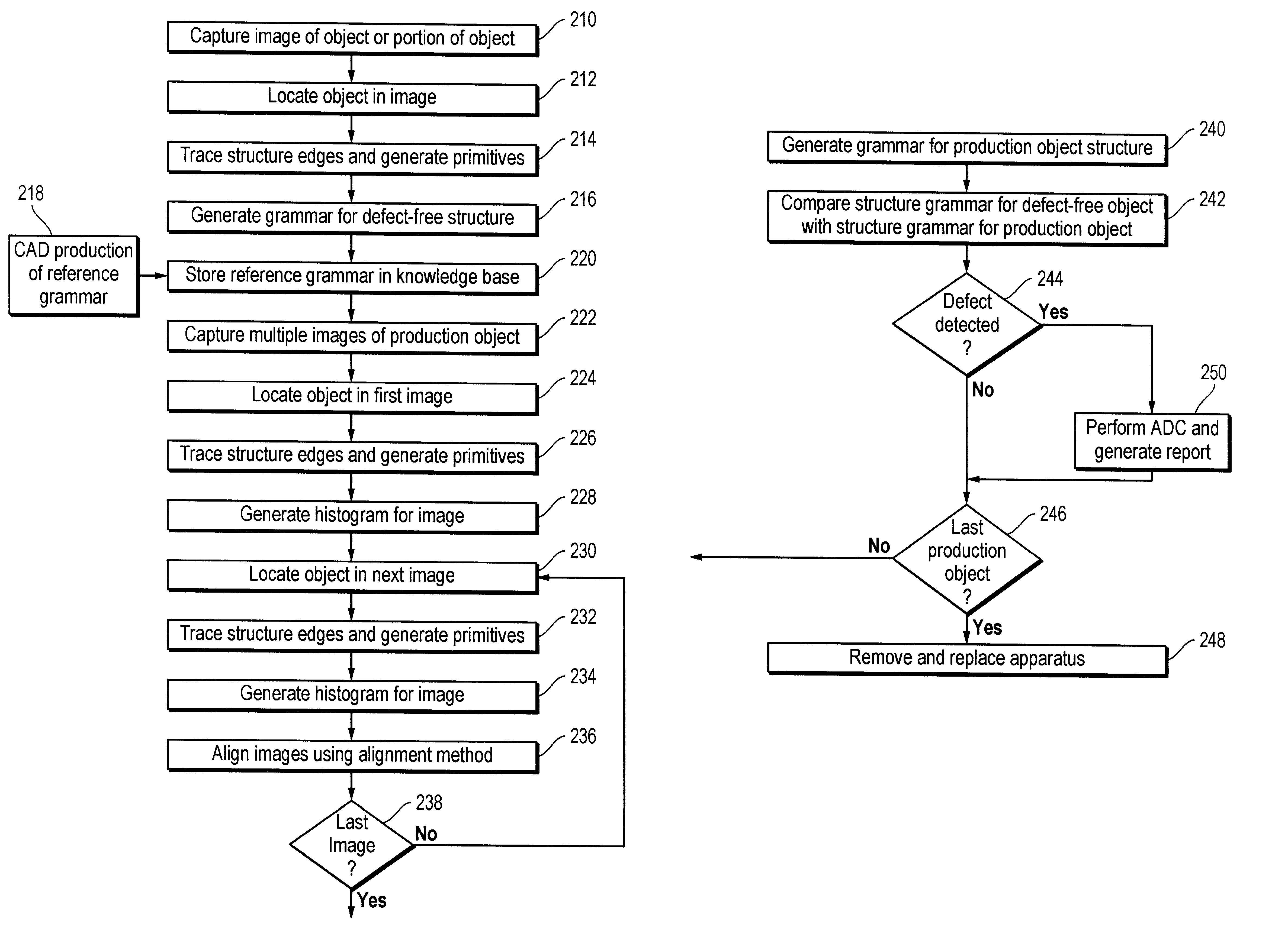
The present invention provides a system and method of optically inspecting structures on the surface of an object. The preferred embodiment is described as a system and method of optically inspecting photoresist structures on the surface of semiconductor wafer dice, and reliably tracing the edges of these structures. Accordingly, the present invention detects and measures the lengths of structure edges. By utilizing image structure grammars (i.e., sets of high level descriptors describing entire structures), the present invention is faster than, and solves the problems associated with, prior art optical inspection techniques.

Anomaly Detection / Location System

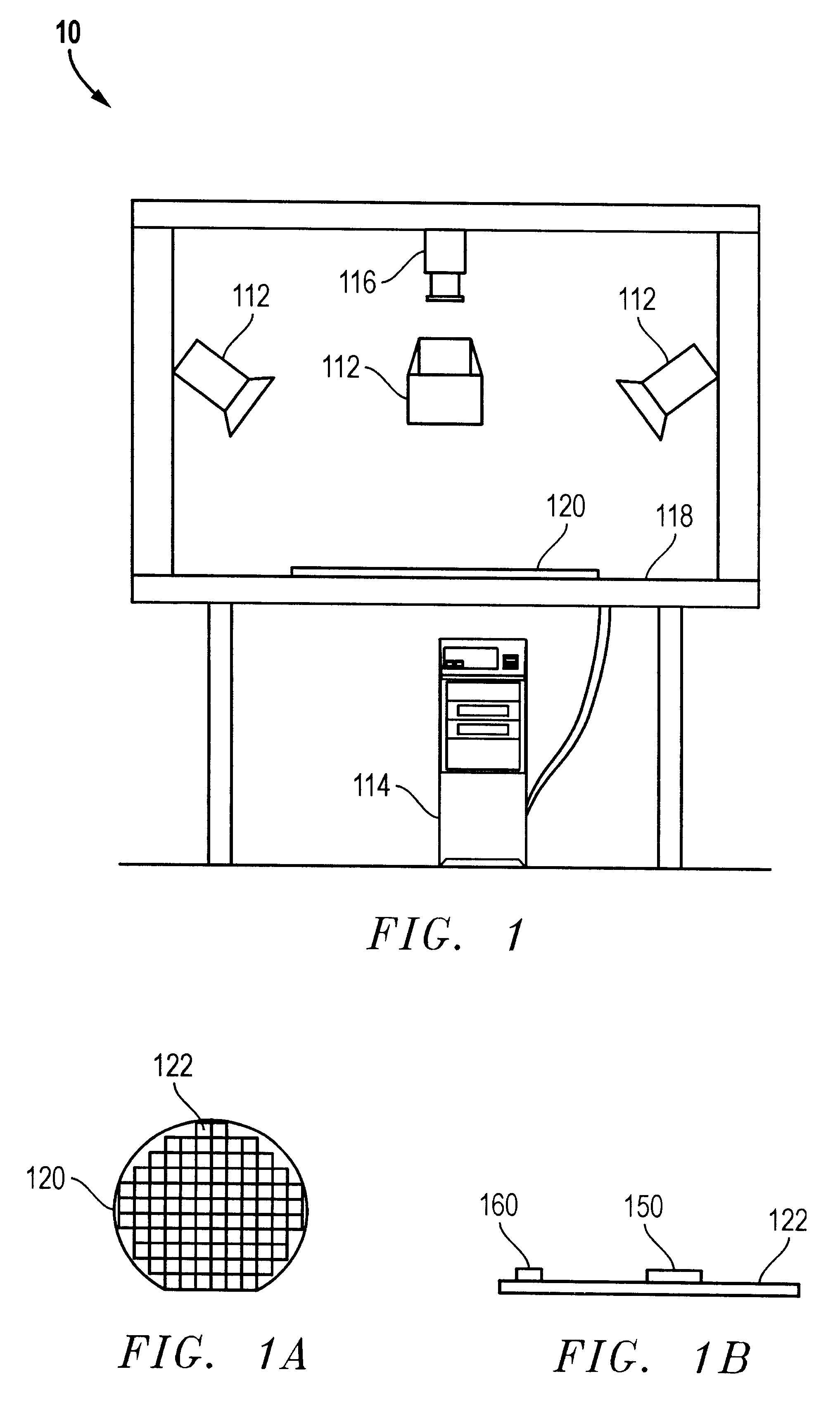
FIG. 1 is a front view of the system of the present invention in an embodiment for inspecting semiconductor wafers. The system 10 may be utilized to detect and locate photoresist anomalies. The anomaly detection / location system 10 comprises light sources 112, a control computer 114, an image capturing device 116, and a wafer supp...


PUM


Abstract

A system and method of optically inspecting a structure on a surface of a production object which is supported on a moving inspection platform. The method reliably traces structure edges and stores structure and structure island characteristics. The system uses a camera and a light or energy source to sharply delineate the structure edges. A sequence of images of the object and the structure are captured, and the structure is detected in each image. The structure is then symbolically decomposed into primitives, and a histogram is produced for each image identifying the slope and length of each edge of the structure. The histograms are compared in each image, and are aligned to eliminate differences due to wobble of the inspection platform or differences in magnification. A production structure grammar is then produced from the aligned images. The production structure grammar is compared to a reference structure grammar generated from a defect-free object. Differences in the two grammars, if any, are used to identify missing, misaligned, or misoriented structures on the production object, and to detect foreign objects and other defects.

Description

1. Technical Field of the InventionThe present invention relates to the inspection of structures on an object and, more specifically, to a system and method for optically inspecting structures on an object.2. Description of Related ArtAn example of a useful application of the present invention is the inspection of semiconductor wafers (wafers) during and after the manufacturing process. In order to transform a wafer into a microprocessor or other electronic device, the wafer undergoes several manufacturing steps. First, a wafer is cut from a crystal ingot (such as crystallized silicon), and an expitaxial layer (a single layer of silicon crystals) is then grown thereon. The creation of an expitaxial layer is often followed by the growth of high quality oxides on the wafer surface, in a process called oxidation. Next, the wafer undergoes several fabrication steps. Each fabrication step places a layer of ions, or other materials, in the wafer or on the wafer in a predetermined geometri...

Claims


Application Information

Patent Timeline
Patent Type & Authority Patents(United States)
IPC IPC(8): G06K9/62
CPCG06K9/626G06T7/001G06T2207/30148G06F18/24765
Inventor HENNESSEY, KATHLEENLIN, YOULING
Owner RUDOLPH TECHNOLOGIES INC
Learn More