
Method for the packaging of electronic components

a technology for electronic components and packaging, applied in the directions of packaging, transportation and packaging, wrapping, etc., can solve the problems of affecting the propagation of surface acoustic waves, the method is not directly applicable to surface-wave components, and the resin alone is not sufficient to protect against external attack from agents such as moistur

Inactive Publication Date: 2002-12-10
THOMSON CSF SA
View PDF16 Cites 201 Cited by
  • Summary
  • Abstract
  • Description
  • Claims
  • Application Information

AI Technical Summary

Benefits of technology

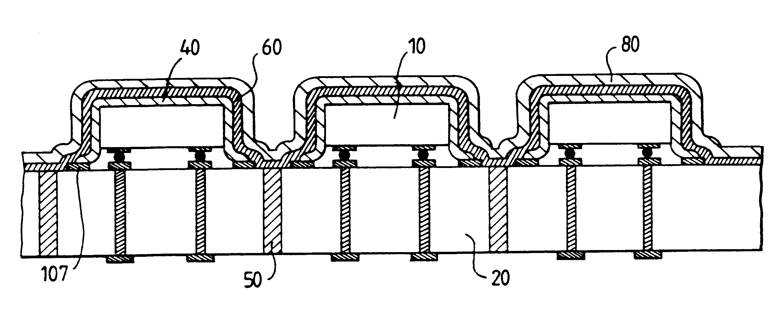
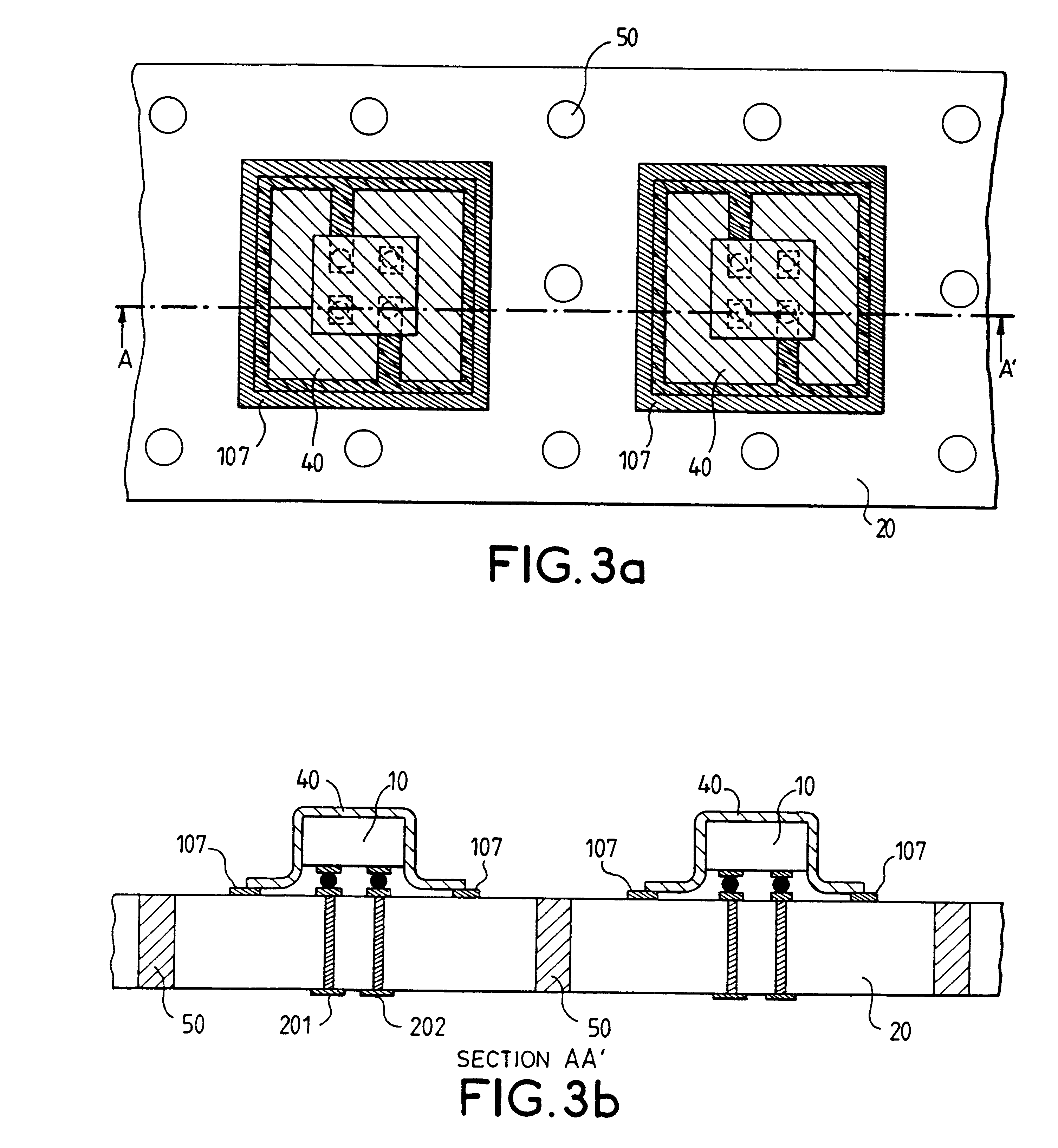
According to one variant of the invention, the method of the invention may furthermore include a step for the total elimination of the film on the base in the zone between the chips enabling the mineral deposit to totally sheath the component and thus provide perfect hermetic sealing quality. In the case of a metal deposit, this step also provides for the resumption of an electrical ground contact on the substrate and thus provides for efficient electromagnetic shielding.

Problems solved by technology

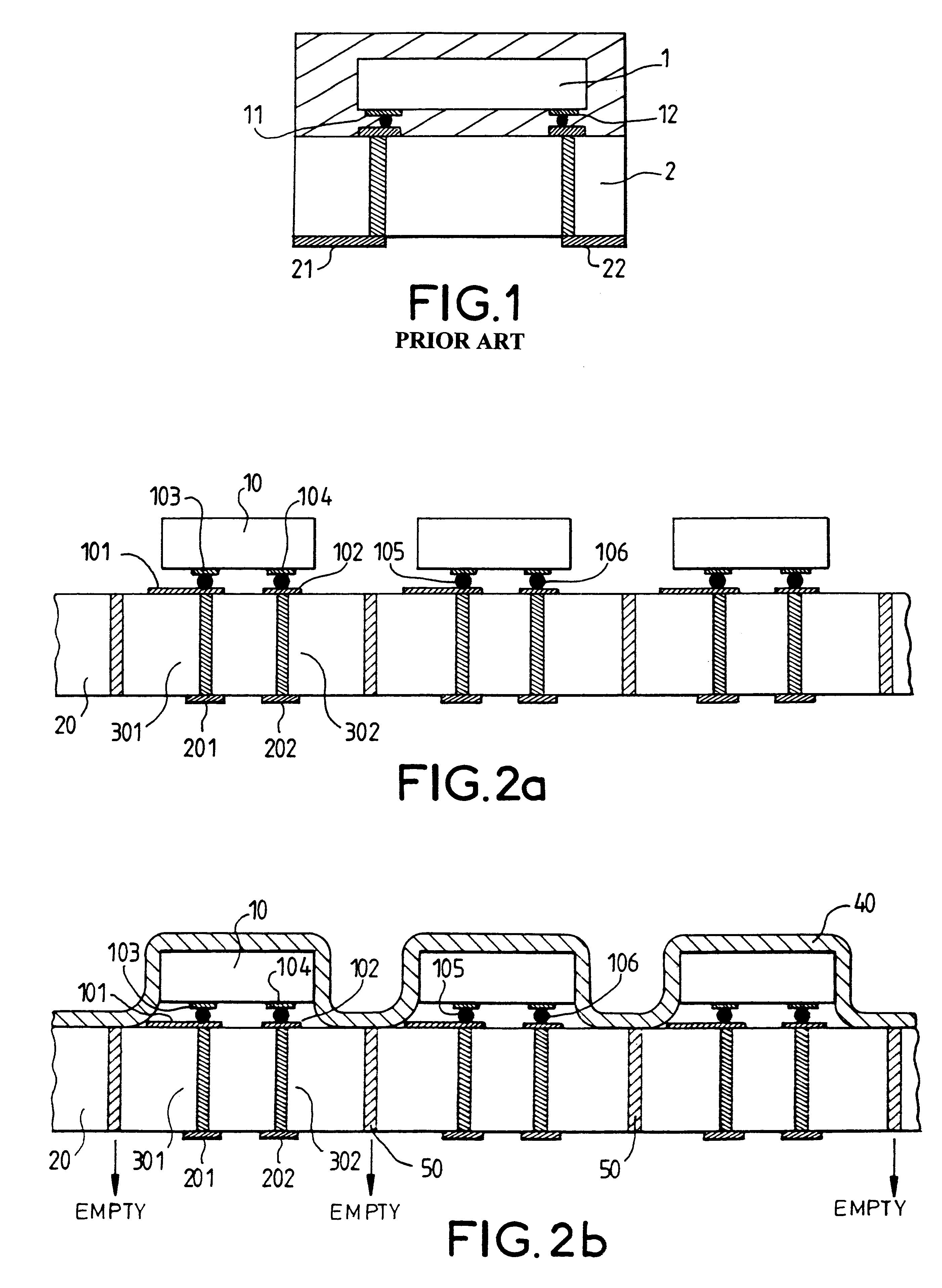
However, this method is not directly applicable to surface-wave components: the encapsulation resin fills the interstice between the component and the base.
This disturbs the propagation of the surface acoustic waves.
Secondly, since the active surface is not passivated, unlike the semiconductor components, the resin by itself is not a sufficient barrier against external attack from agents such as moisture.
In the case of a plastic sheet, even if it is metallized, the shielding is neither hermetically sealed nor perfectly shielded.

Method used


Image

  • Method for the packaging of electronic components
  • Method for the packaging of electronic components
  • Method for the packaging of electronic components

Examples


Embodiment Construction

We shall describe a method for the batch manufacture of packaged electronic components especially suited to the case of surface acoustic wave components for which it is imperative to preserve a free space for the propagation of the acoustic waves.

The method of manufacture comprises a first step illustrated in FIG. 2a in which the components 10 are mounted, in a batch, on a board 20. This board has the connection pads 201 and 202 on one of its faces called an external face and connection pads 101 and 102 on the face opposite the external face. The latter pads 101 and 102 are used to connect the exterior of the electrical contacts 103 and 104 of the components 10 by "flip-chip" type mounting by means of first conductive via holes 301, 302 and intermediate conductive elements 105, 106. These intermediate conductive elements may be metal balls made of gold or they may be solder balls. The electrical contact operation may be done by thermocompression, bonding or ultrasonic soldering.

In a...


PUM

PropertyMeasurementUnit
thicknessaaaaaaaaaa
pressureaaaaaaaaaa
conductiveaaaaaaaaaa

Abstract

A method for the packaging of electronic components, including the mounting of at least one electronic component on its active face side to a base, the base including electrical contacts on an external face and connection pads on a face opposite the external face, and including a first series of via holes connecting the electrical contacts and the connection pads and a second series of holes for use in aspiration. A deformable film is deposited on the face opposite to the active face of the electronic component or components. The deformable film is aspirated through the second series of holes from the face opposite the external face of the base, so as to sheath the electronic component or components. The method may furthermore include, on top of the deformable film, a mineral deposition to provide for the hermetic sealing of the components and a conductive deposition to provide for the shielding. Such an application may find particular application to surface wave filters.

Description

1. Field of the InventionThe present invention relates to the packaging of electronic components, especially components whose surface needs to be unoccupied such as surface acoustic wave (SAW) filters, RF components, sensors and, more specifically, the method for making a packaging of this kind.Surface wave components (SWC) used in electronics, especially as filters in the radiofrequency domains or intermediate frequency domains, in order to select frequency bands in mobile telephony, make use of the principle of the generation and propagation of acoustic waves on the surface of a piezoelectric substrate. This function makes it necessary to prepare a free space on the surface of the component on which the acoustic waves are propagated. Thus, the standard methods for the protection of surface acoustic wave components use hermetically sealed ceramic or metal packs. However, these methods are costly and unproductive, and make it difficult to minituarize the components.2. Description of...

Claims


Application Information

Patent Timeline
Patent Type & Authority Patents(United States)
IPC IPC(8): H01L21/02H01L23/31H01L21/56H01L23/28H03H3/08H03H3/00B65B11/00H01L23/02H01L23/00H01L23/552H03H9/25
CPCH01L21/56H01L23/3135H01L23/3164H01L23/552H01L24/97H03H3/08H01L21/561H01L2224/16235H01L2224/97H01L2924/01004H01L2924/01005H01L2924/01027H01L2924/01033H01L2924/01057H01L2924/01058H01L2924/01079H01L2924/15151H01L2924/3025H01L2224/73253H01L2224/16225H01L2924/0102H01L2224/81H01L2924/181H01L2224/05573H01L2224/05568H01L2924/00014H01L2224/05599H01L2924/00012B65B11/00
Inventor BUREAU, JEAN-MARCELZIERE, JACQUESLE BAIL, DANIELLELONG, CHRISTIANNGUYEN, NGOC-TUAN
Owner THOMSON CSF SA
Learn More