Wafer level interconnection
a technology of electronic components and wafers, applied in the field of rf mems (microelectromechanical systems), can solve the problems of many hetero-junction technologies, epitaxial methods, and substrate materials that are considered incompatible with rf mems fabrication technology, and the rf performance of the circuit can be limited,
- Summary
- Abstract
- Description
- Claims
- Application Information
AI Technical Summary
Problems solved by technology
Method used
Image
Examples
Embodiment Construction
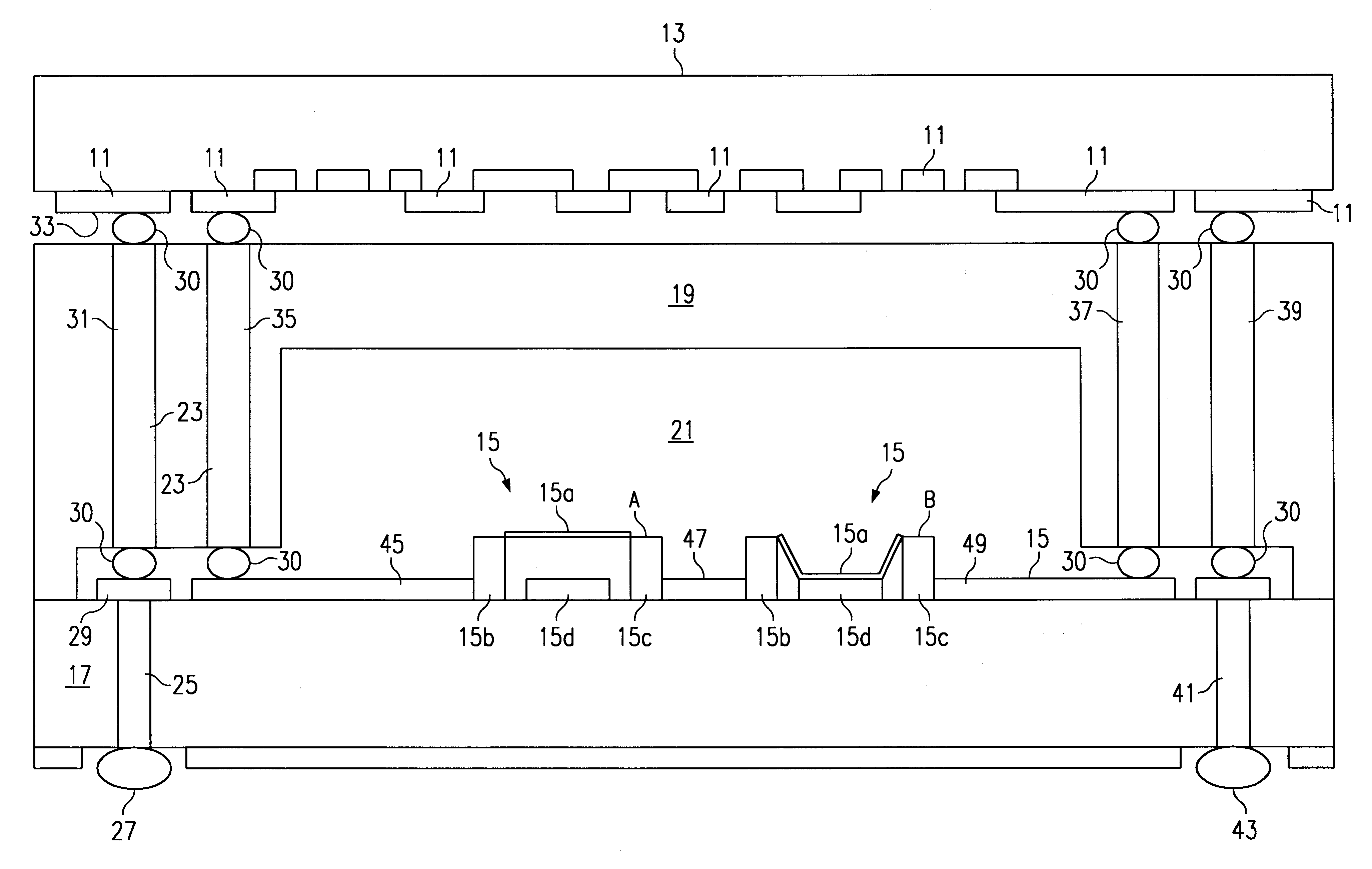
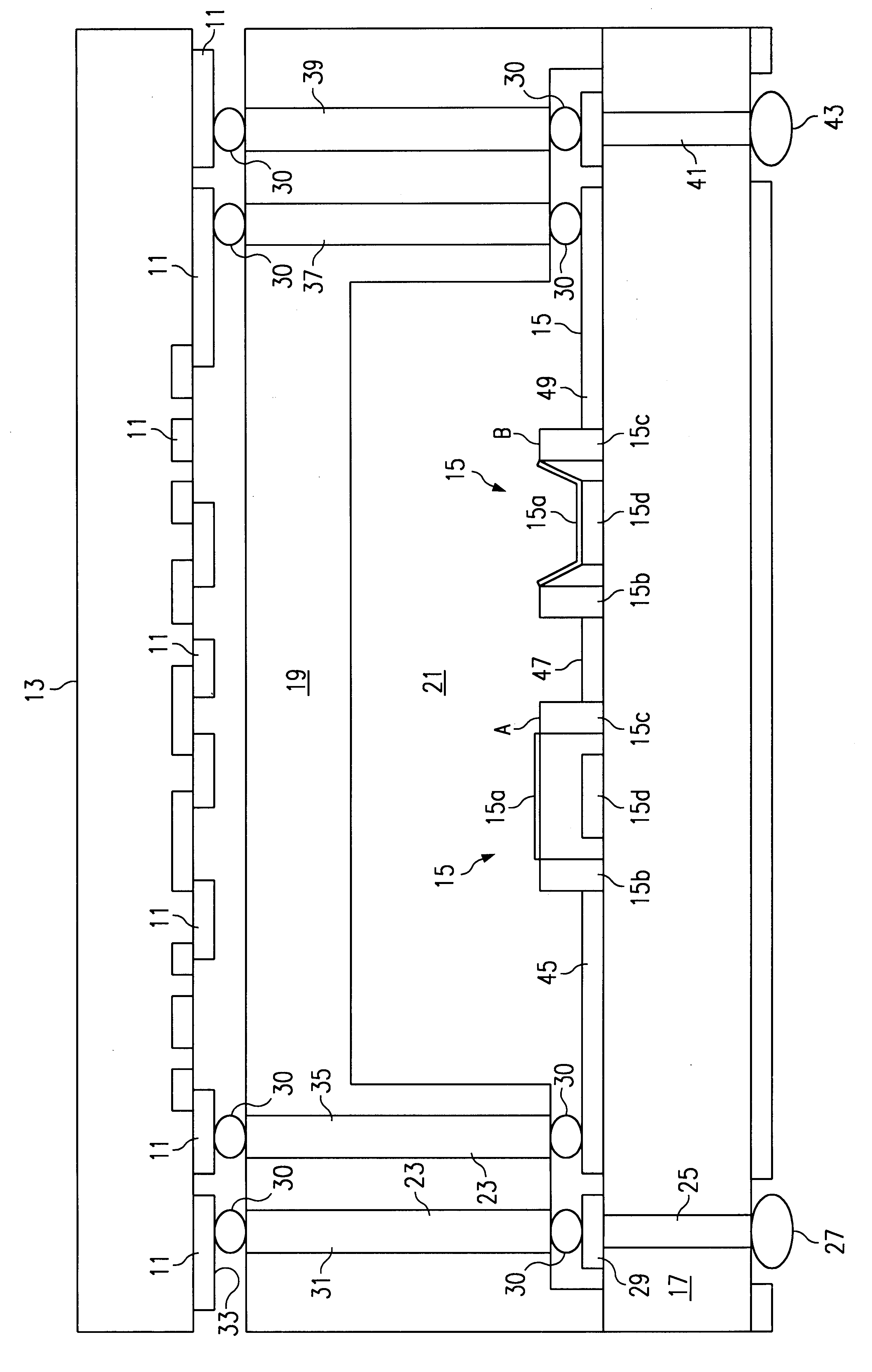
According to one embodiment of the present invention illustrated in FIG. 1 vertical electrical interconnection between the electronics circuitry 11 on one low-resisitvity SiGe substrate 13 and RF MEMS circuitry 15 on a separate high resistivity silicon (HR) substrate 17. The low-resistivity substrate material 13 may also be silicon CMOS or gallium arsenide (GaAS) substrate. This is accomplished by using wafer fabrication techniques to construct a conductive metallization layer on either the primary (i.e., RF MEMS) substrate 17 or the secondary (i.e., other electronics) substrate 13. A dielectric lid 19 is spaced between the electronics circuitry 11 on the substrate 13 and the high resistivity substrate 17 and provides a canopy or lid over the RF MEMS circuitry 15 leaving a gap 21 over the RF MEMS circuitry 15. The gap 21 is filled with an inert environment such as a gas such as nitrogen or a vacuum. The lid 19 may be made of Pyrex,quatrz or glass and is made of a material with the s...
PUM
 Abstract
Description
Claims
Application Information

