Method for producing a copper connection

a copper connection and copper technology, applied in the direction of solid-state device manufacturing, electric devices, semiconductor/solid-state device manufacturing, etc., can solve the problems of inability to use cleaning processes, inability to clean, and inability to penetrate the layer of "low-k" material, so as to prevent contamination of dielectric material and reinforce mechanical rigidity of the structure

Inactive Publication Date: 2003-02-18
COMMISSARIAT A LENERGIE ATOMIQUE ET AUX ENERGIES ALTERNATIVES +1
View PDF10 Cites 29 Cited by
  • Summary
  • Abstract
  • Description
  • Claims
  • Application Information

AI Technical Summary

Benefits of technology

The protective layer that remains on the walls of the hole prevents contamination of the dielectric material. It makes it possible for the connection hole to be cleaned without any risk. It reinforces the mechanical rigidity of the structure. It is also advantageous if spacers are used, providing they do not act as a barrier to the diffusion of the copper.

Problems solved by technology

The second harmful effect consists in a pollution of the surface of the connection element 2 as a function of the type of chemistry used in the etching process.
When the dielectric material of the damascene structure is a "low-k" material, several problems arise.
As the copper is sprayed after etching the encapsulation layer, it may cause in-depth contamination of the layer of "low-k" material (in the case of a polymer or a porous material).
The cleaning processes may not be able to be used because of the risk of attack, or even deterioration, of the dielectric material that these processes may cause.
Moreover, these cleaning processes do not allow decontamination of the bulk of dielectric material.
At this moment in time, there is no cleaning solution for SiLK.
In addition, the use of "low-k" material generally causes problems in the mechanical resistance of the structures.

Method used


Image

  • Method for producing a copper connection
  • Method for producing a copper connection
  • Method for producing a copper connection

Examples


Embodiment Construction

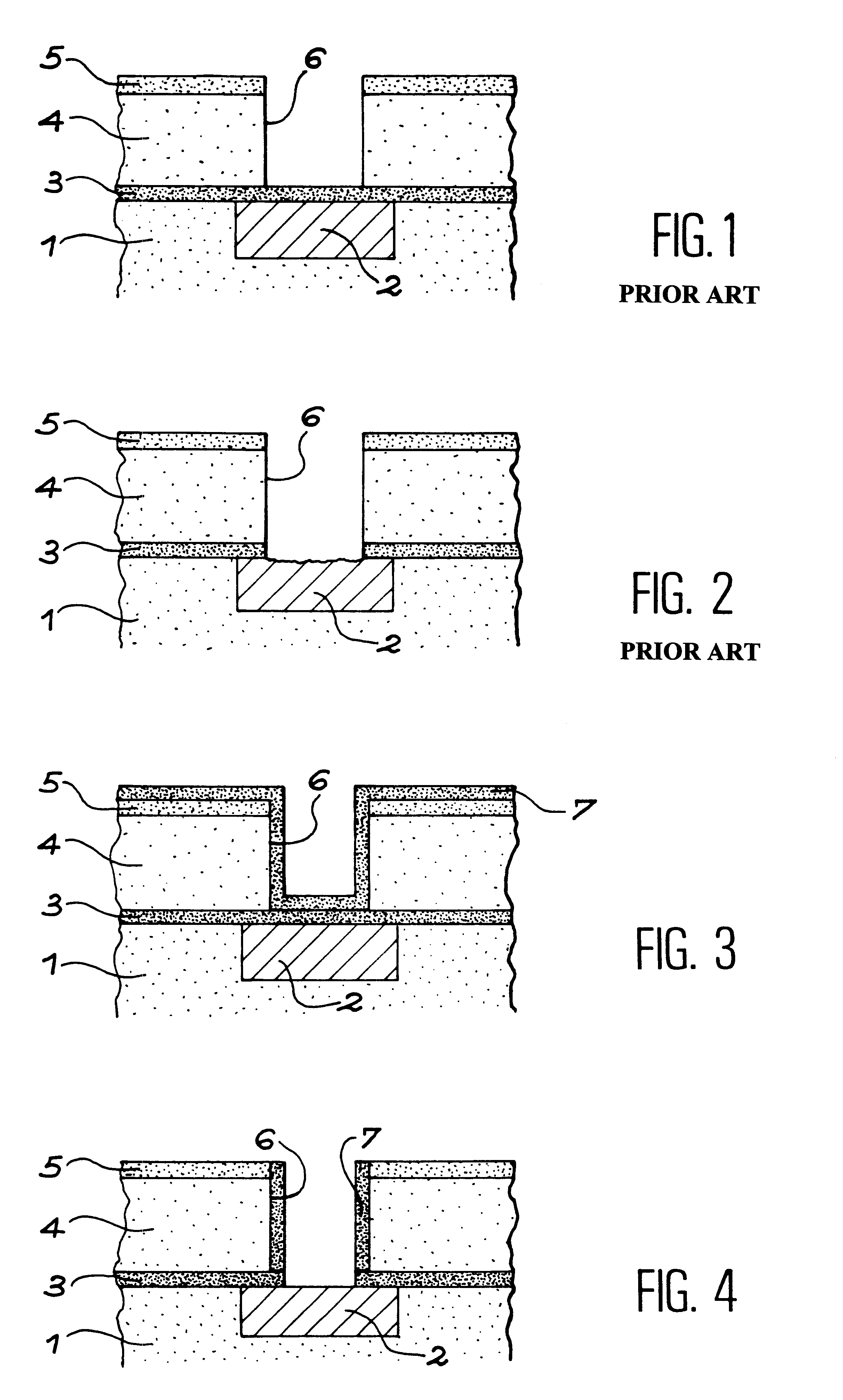
The invention provides a solution to the problems described above.

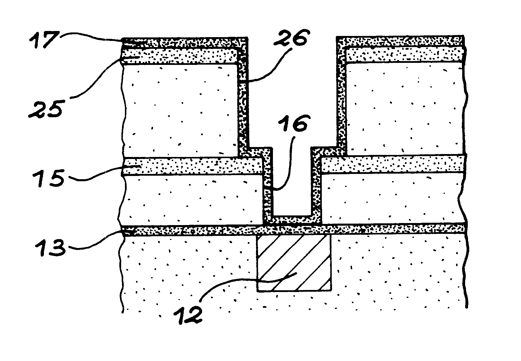
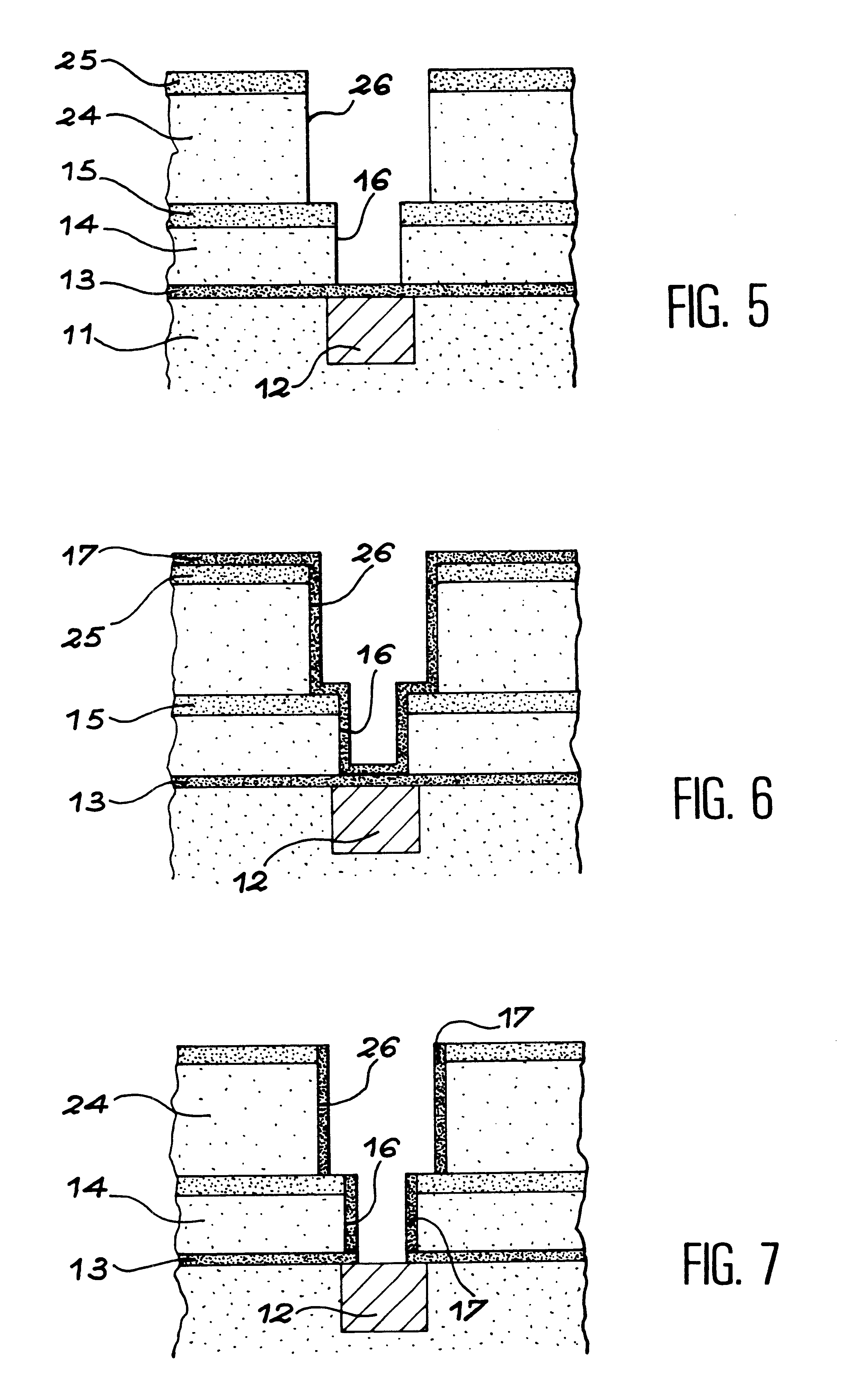
The object of the invention is a process for making a copper connection with a copper connection element in an integrated circuit comprising a damascene structure, with the connection element being covered successively with an encapsulation layer and at least one layer of dielectric material with a very low dielectric constant (called a "low-k" material), the process comprising the following steps:

etching said layer of dielectric material until the encapsulation layer is reached in order to obtain a connection hole, opposite the connection element,

forming a protective layer on the walls of the connection hole, with the protective layer enabling contamination of the layer of dielectric material by diffusion of copper to be avoided,

etching the encapsulation layer, at the bottom of the connection hole, in such a way as to reveal the connection element,

filling the connection hole with copper.

The protective layer that rema...


PUM

PropertyMeasurementUnit
relative permittivityaaaaaaaaaa
dielectric constantaaaaaaaaaa
metallicaaaaaaaaaa

Abstract

The invention relates to a process for making a copper connection with a copper connection element in an integrated circuit comprising a damascene structure, with the connection element being covered successively with an encapsulation layer and at least one layer of dielectric material with a very low dielectric constant. The process includes the steps of etching the layer of dielectric material until the encapsulation layer is reached in order to obtain a connection hole opposite the connection element. A protective layer is then formed on the walls of the connection hole, with the protective layer preventing contamination of the dielectric layer from diffusion of copper. The protective and encapsulation layers are then etched at the bottom of the connection hole in such a way as to reveal the connection element. The connection hole is then filled with copper.

Description

The present invention concerns a process for making a copper connection through a layer of dielectric material in an integrated circuit.STATE OF THE PRIOR ARTThe improvements in the performance of integrated circuits (speed, low consumption) have required a change in some of the materials that have been used up till now. In order to reduce the capacity that exists between the conductive lines formed in one or several layers of dielectric material (damascene-type structures), it is advantageous to use, as the dielectric material, materials with a very low dielectric constant. These materials, called "low-k" materials, comprise organic materials and porous materials.The improvements in the performance have also been achieved through the use of a metal that is more conductive than aluminium, which has traditionally been used to make the interconnection lines. Copper, whose resistivity is nearly half that of aluminium doped with copper, has shown itself to be the best candidate.FIGS. 1 ...

Claims


Application Information

Patent Timeline
Patent Type & Authority Patents(United States)
IPC IPC(8): H01L21/70H01L21/768H01L23/522H01L23/52H01L21/3205
CPCH01L21/76802H01L21/76807H01L23/5226H01L21/76844H01L21/76831H01L2924/0002H01L2924/00
Inventor MORAND, YVESGOBIL, YVELINEDEMOLLIENS, OLIVIERASSOUS, MYRIAM
Owner COMMISSARIAT A LENERGIE ATOMIQUE ET AUX ENERGIES ALTERNATIVES
Why Eureka
Try Eureka