Supercharge Your Innovation With Domain-Expert AI Agents!

Semiconductor device and its manufacturing method

a technology of semiconductors and manufacturing methods, applied in the direction of sustainable manufacturing/processing, final product manufacturing, printed circuit aspects, etc., can solve the problems of cracks in the junction portion of the external connecting terminal of the printed circuit board, the reliability of mounting the printed circuit board cannot be greatly reduced, and the effect of short tim

Inactive Publication Date: 2003-02-25
TEXAS INSTR INC
View PDF3 Cites 10 Cited by
  • Summary
  • Abstract
  • Description
  • Claims
  • Application Information

AI Technical Summary

Benefits of technology

In this invention, since the forming of the supporting posts for the purpose of the external connecting terminals can be done by carrying and connecting conductive supporting posts to the desired positions of the wiring, supporting posts of the target height can be obtained in an extremely short time compared to that required for forming of supporting posts by means of the plating method used in the past. By this means, a degree of freedom in the design of the supporting posts can be obtained, and in that way, supporting posts of sufficient dimensions, shape, and materials necessary for obtaining mounting reliability for the package can be obtained.

Problems solved by technology

However, even when the package size was decreased, the manufacturing cost could not be lowered very much.
On the one hand, in a wafer level CSP, in the same manner as in a conventional CSP type semiconductor device, there are problems in mounting reliability in relation to the printed circuit board.
In thermal cycle tests of this type of semiconductor device, cracks are generated in the junction portion of the external connecting terminals of the printed circuit board, and there are instances when the junction is open and defective.
(1) Time and expense are required in forming the metallic supporting posts on the main face of the semiconductor chip. In other words, the abovementioned metallic supporting posts are formed by means of accumulating a metal plating (for example, copper plating) on the wiring pattern. In order to relieve the above-mentioned stress, it is necessary for said supporting posts to have a height of more than 100 .mu.m, and more than two hours are required to form these supporting posts by means of the plating method. In order to further improve the mounting reliability for the semiconductor device, it is necessary to further heighten the supporting posts, (for example, to more than 200 .mu.m), and realization of that is extremely difficult from the aspects of time and cost.
(2) In the case of forming the metallic supporting posts by means of a plating method, because their shape and material cannot be freely selected, the degree of freedom for the design of the target package is limited.

Method used


Image

  • Semiconductor device and its manufacturing method
  • Semiconductor device and its manufacturing method
  • Semiconductor device and its manufacturing method

Examples


Embodiment Construction

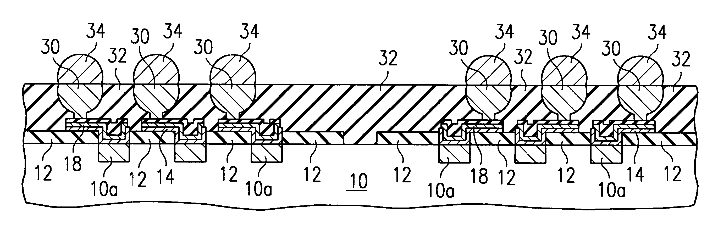
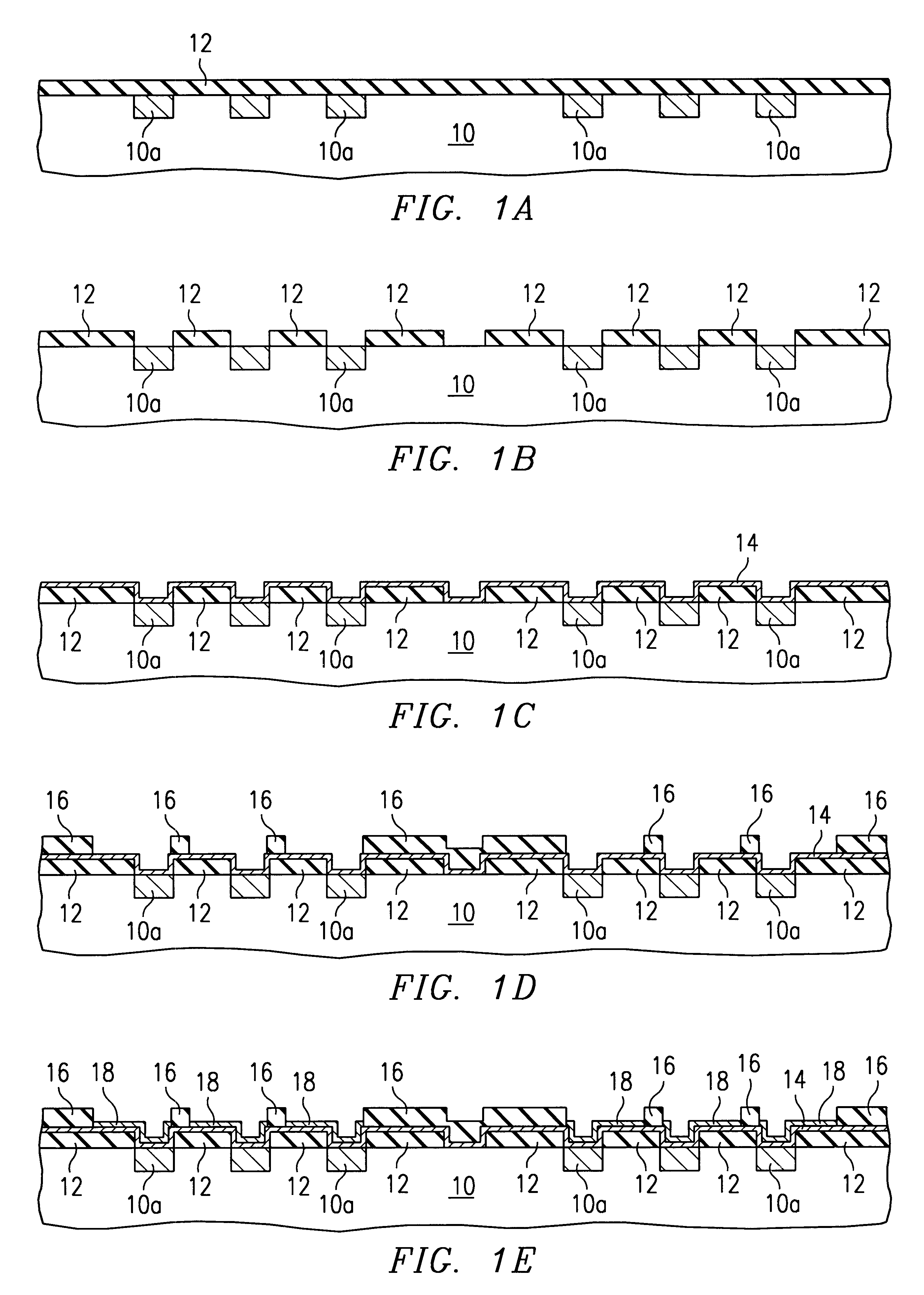
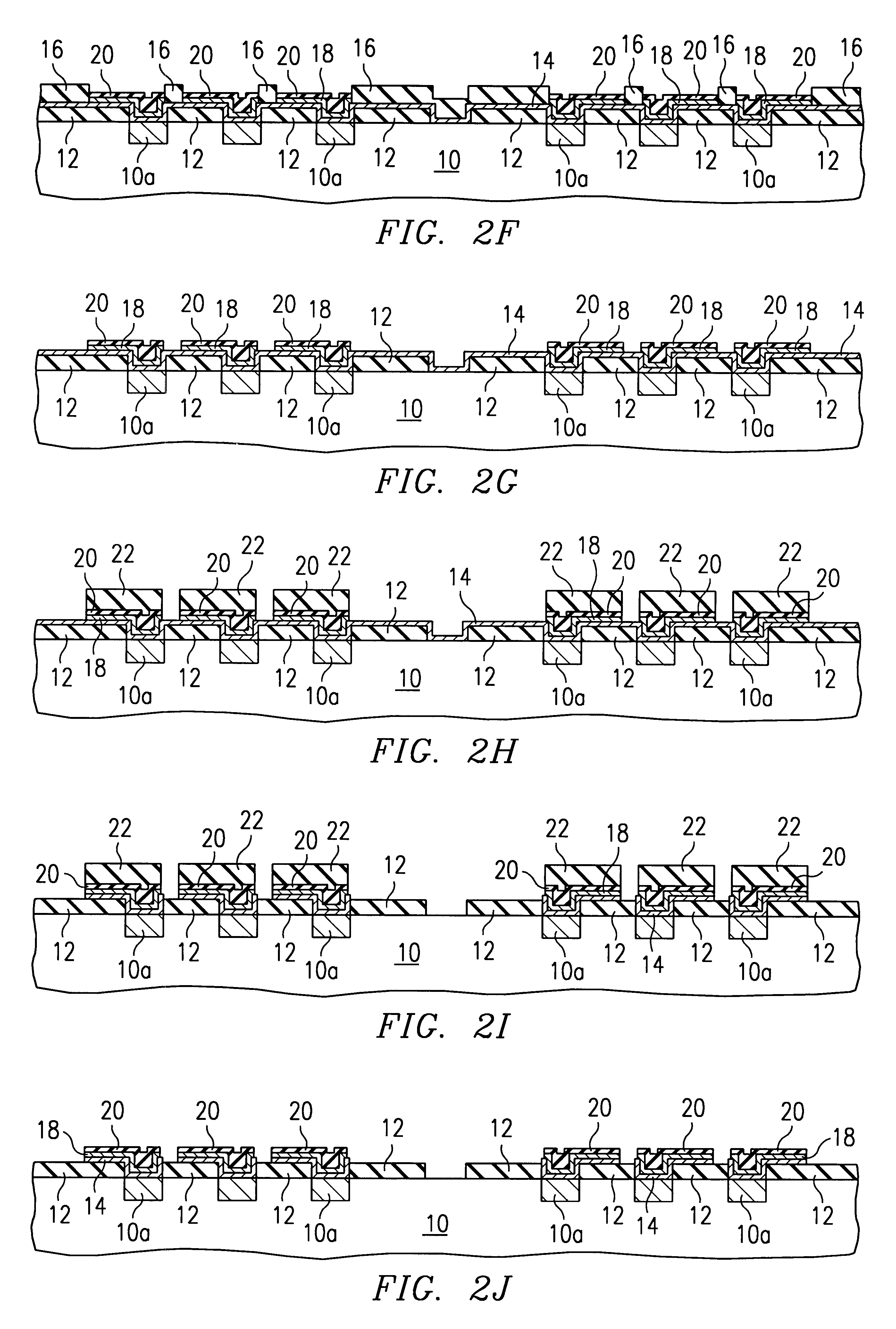
Below, an embodiment of this invention will be explained using figures. In the manufacturing method for a semiconductor device related to this embodiment, a package process is executed for a wafer on which semiconductor elements are formed, and finally, a packaged semiconductor device is obtained when the wafer is diced The manufacturing method related to this embodiment configuration contains processes that execute necessary wiring on the surface of a wafer on which semiconductor elements are formed, connect conductive balls that are prepared by a separate process beforehand on top of this, cover the wafer surface with resin, move solder balls that are external connecting terminals, and produce individual packages by dicing the wafer along the boundary lines of the semiconductor elements. These specific processes are sequentially explained by following FIG. 1(A) to FIG. 4(R). A person within this industry probably understands that these figures are shown in an exaggerated form for ...


PUM


Abstract

Improve the productivity and cost for the manufacturing of a semiconductor device referred to as a wafer level CSP. The manufacturing method for a semiconductor device related to this invention contains each of the processes that form a wiring (18) for the purpose of electrically connecting each electrode pad (10a) and external connecting terminals on top of a wafer (10) on which semiconductor elements are formed, connect conductive balls that are preformed by a separate process on top of this, and next, cover the above-mentioned wafer with a resin (32) such that the upper portion of the conductive supporting posts (30) are exposed. In a later process, solder balls (34) are arranged as external connecting terminals on the upper portion of the conductive supporting posts, and in the final process, semiconductor elements are formed by dicing the above-mentioned wafer along the boundary lines of the above-mentioned semiconductor elements.

Description

This invention relates to a semiconductor device of the so-called wafer level CSP type and its manufacturing method in which the packaging of a semiconductor chip is realized in the wafer state.In the semiconductor device manufacturing industry, efforts are continuing for the purpose of further downsizing a single package semiconductor device. The initial effort for the purpose of realizing miniaturization of a semiconductor device reduced the size of the semiconductor chip itself. By making the semiconductor chip smaller, the number of chips that could be obtained from one wafer was increased, and along with bringing down manufacturing costs, since the movement distance of electrons between each element could be made shorter, the operating speed was increased. Due to the development of microscopic processing technology, decreasing the chip size for a semiconductor device having the same functions became possible. The current leading-edge design guideline is less than 0.18 .mu.m, an...

Claims


Application Information

Patent Timeline
Patent Type & Authority Patents(United States)
IPC IPC(8): H01L21/02H01L23/485H01L21/60H01L21/56H01L23/48H05K3/34
CPCH01L21/56H05K3/3436H01L24/11H01L24/13H01L2224/11334H01L2224/131H01L2924/01002H01L2924/01015H01L2924/01022H01L2924/01029H01L2924/01046H01L2924/01061H01L2924/01074H01L2924/01075H01L2924/01078H01L2924/01079H01L2924/01082H05K2201/0379H05K2201/10234H05K2201/10977H01L2924/014H01L2924/01033H01L2924/01024H01L2924/00013H01L2924/01005H01L2924/01006H01L2924/01019H01L2224/13099H01L24/03H01L24/05H01L2224/023H01L2224/05001H01L2224/05008H01L2224/05024H01L2224/05026H01L2224/05184H01L2224/05548H01L2224/05569Y02P70/50H01L2224/05644H01L2924/00014H01L2224/05664H01L2224/05147H01L2224/05155H01L2224/05166H01L2224/05171H01L2924/0001
Inventor MURATA, KENSHOMASUMOTO, MUTSUMIMASUMOTO, KENJI
Owner TEXAS INSTR INC
Features
  • R&D
  • Intellectual Property
  • Life Sciences
  • Materials
  • Tech Scout
  • Unparalleled Data Quality
  • Higher Quality Content
  • 60% Fewer Hallucinations
Learn More