Nanotube junctions

Inactive Publication Date: 2003-03-25
RGT UNIV OF CALIFORNIA
View PDF7 Cites 79 Cited by
  • Summary
  • Abstract
  • Description
  • Claims
  • Application Information

AI Technical Summary

Benefits of technology

It is an object of the invention to design carbon nanotubes containing adjacent sections of differing electrical properties. These nanotubes can be constructed from combinations of carbon, boron, nitrogen and other elements. It is a further object of the invention to design carbon nanotubes in which the nanotube index is different on either side of a junction point in the tube so that the electrical properties on either side of the junction vary in a useful fashion. For example, a carbon nanotube may be electrically

Problems solved by technology

Since defects can change the index in a nanotube, they are considered to be the cause of some flaring

Method used


Image

  • Nanotube junctions
  • Nanotube junctions
  • Nanotube junctions

Examples


example 1

TEM of Junction Nanotube

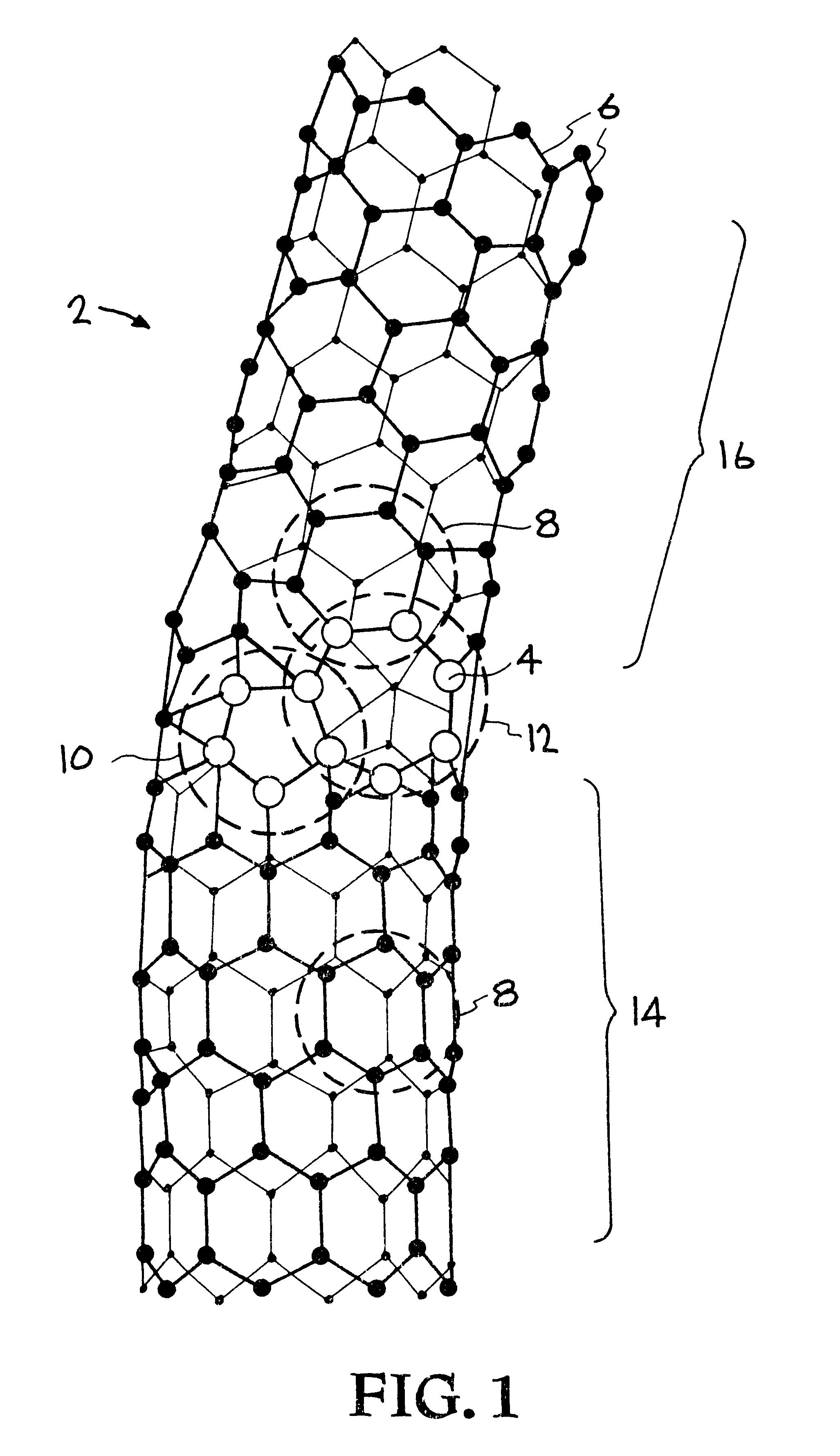
FIG. 2 shows a transmission electron microscope photograph of the inventive carbon nanotube having an extended pehtagon-heptagon pair in the junction. The interior wall of the tube 20 is darkened for photographic clarity. The positions of a heptagon 22 and pentagon 24 were inferred by performing geometrical constructions and noting the locations at which tubes with parallel walls join the junction 26. This carbon nanotube was synthesized, isolated, and imaged via transmission electron microscopy using conventional experimental methods [S. Iijima, Nature 354, pgs. 56-58, (1991)].

Tubes can also be created which have more than one concentric wall. These tubes are known as multiwalled tubes. FIG. 2 shows a multiwalled tube. The parallel strips above the interior wall 20 are cross-sectional cuts of many concentric tubes. Multiwalled tubes can be designed with junctions as described above existing in the individual walls, yielding structures with transitions in ove...

example 2

Semiconductor / metal Junction

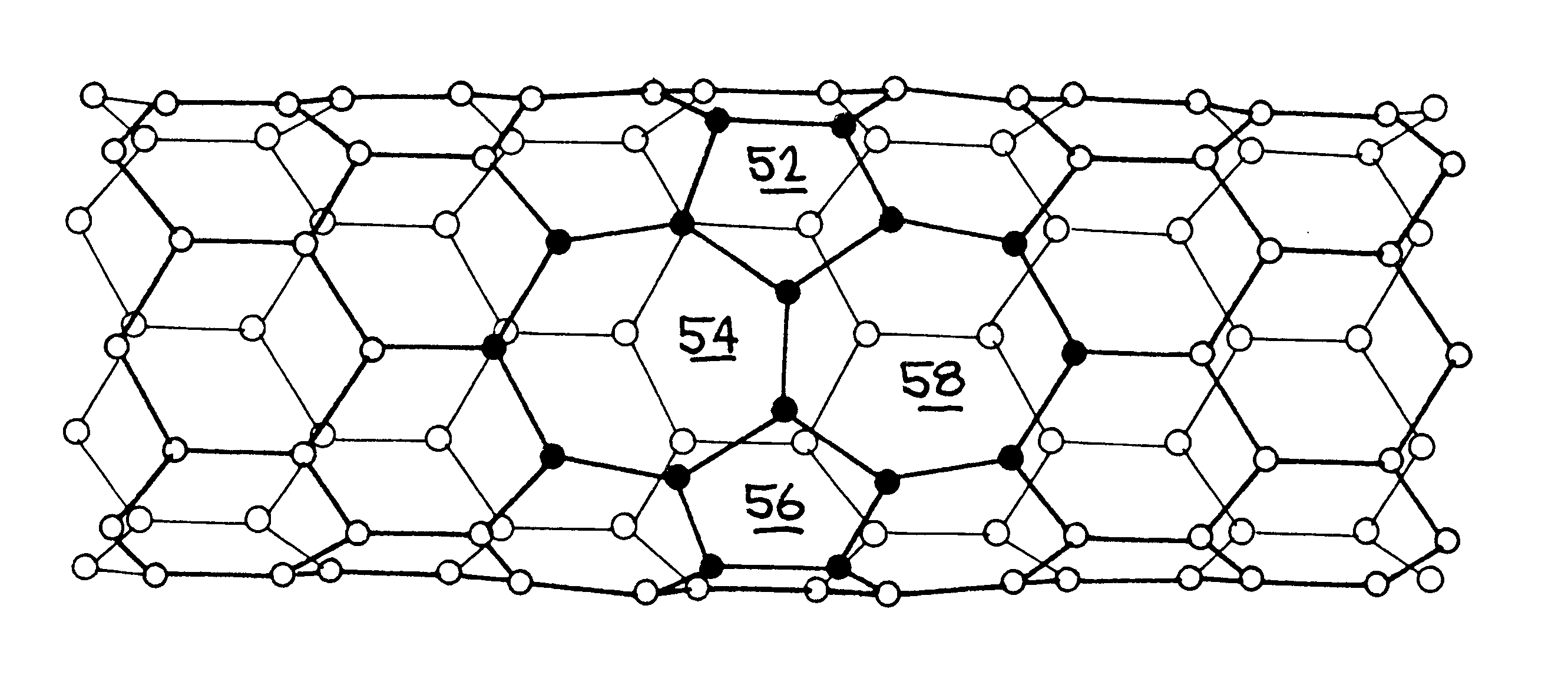
FIG. 1 shows an (8,0) carbon nanotube joined to a (7,1) carbon nanotube. The circled atoms 10 and 12 comprise the adjacent pentagon-heptagon pair that forms the junction. The structure can be denoted as (8,0) / (7,1) in analogy with interfaces of bulk materials. By calculating the electronic structure using quantum theory we find that far from the interface the (7,1) section is a semimetal and the (8,0) section is a semiconductor having a moderate band-gap. The two sections and the junction combine to form a quasi one-dimensional semiconductor / metal junction, taking into account that the band-gap is small enough in the (7,1) nanotube section that it approximately behaves like a metal. The inventive structure, un like other semiconductor / metal junctions, is essentially composed of a single chemical element.

A tight quantum-based tight-binding model having one .pi.-orbital per atom along with the Surface Green Function Matching method (SGFM) (F. Garcia-Moliner...

example 3

Semiconductor / semiconductor Junction

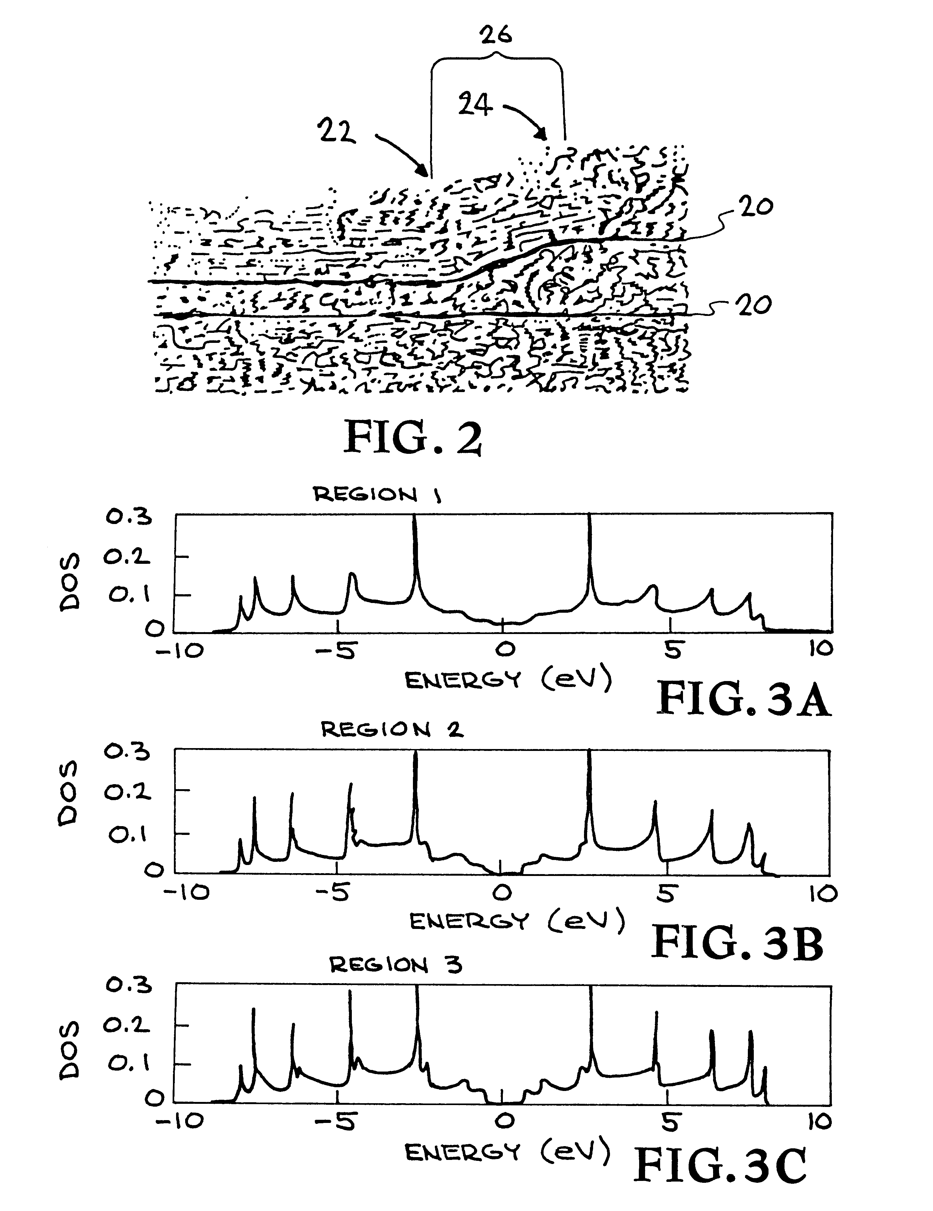
A (8,0) / (5,3) semiconductor / semiconductor carbon nanotube was examined using the same techniques as above. The heterojunction joining the unit cells of the (8,0) and (5,3) nanotube sections was formed using three pentagon-heptagon pairs and two hexagons. Two different junction configurations were possible: one having the two hexagons adjacent and one having the hexagons separated. The sequence of n-membered carbon rings encountered when tracing around the circumference of the nanotube heterojunction was: 6, 7, 5, 6, 7, 5, 7, 5.

The band-gap of a defect-free (5,3) nanotube is 1.4 eV 0.2 eV larger than that of the (8,0) nanotube. The (8,0) / (5,3) nanotube thus provides a prototypical example of a semiconductor / semiconductor heterojunction.

The methods used to determine the LDOS was the same as described in Example 2.

The results for the (8,0) / (5,3) semiconductor-semiconductor heterojunction are plotted in FIGS. 5 and 6. For the same reasons of compariso...


PUM


Abstract

The present invention comprises a new nanoscale metal-semiconductor, semiconductor-semiconductor, or metal-metal junction, designed by introducing topological or chemical defects in the atomic structure of the nanotube. Nanotubes comprising adjacent sections having differing electrical properties are described. These nanotubes can be constructed from combinations of carbon, boron, nitrogen and other elements. The nanotube can be designed having different indices on either side of a junction point in a continuous tube so that the electrical properties on either side of the junction vary in a useful fashion. For example, the inventive nanotube may be electrically conducting on one side of a junction and semiconducting on the other side. An example of a semiconductor-metal junction is a Schottky barrier. Alternatively, the nanotube may exhibit different semiconductor properties on either side of the junction. Nanotubes containing heterojunctions, Schottky barriers, and metal-metal junctions are useful for microcircuitry.

Description

I. BACKGROUND OF THE INVENTION1. Field of the InventionThis invention relates generally to microelectronics and more specifically to metal-semiconductor, metal-metal, and semiconductor-semiconductor junctions in nanotubes.2. Description of Related ArtThe electronic structure of carbon nanotubes is governed in part by the geometrical structure of the tube (R. Saito et al., Appl Phys Lett, 60:2204, 1992; and N. Hamada et al., Phys Rev Lett. 68:1579, 1992).A nanotube index (n,m) has been developed to describe the nanotube structure. It is described in detail by C. T. White et al. "Predicting Properties of Fullerenes and their Derivatives", Chapter 6, page 159 and following, in Buckminsterfullerenes, W. E. Billups, and M. A. Ciufolini, ed. (NY: VCH Publishers, 1993). Carbon nanotubes can be understood by thinking of them as a graphite sheet, in which the carbon atoms are arranged in a honeycomb lattice of hexagonal rings. The sheet is rolled up and spliced together to form a tube. That ...

Claims


Application Information

Patent Timeline
IPC IPC(8): D01F9/12
CPCB82Y30/00D01F9/12Y10T428/30Y10S977/734Y10S977/848Y10S977/742
Inventor CRESPI, VINCENT HENRYCOHEN, MARVIN LOULOUIE, STEVEN GWON SHENGZETTL, ALEXANDER KARLWALTER
Owner RGT UNIV OF CALIFORNIA
Why Eureka
Try Eureka