Automatic gain control circuit with high linearity and monotonically correlated offset voltage

a gain control and offset voltage technology, applied in the direction of automatic tone/bandwidth control, gain control, amplifier modification to reduce non-linear distortion, etc., can solve the problems of inability to adjust the input signal, and inability to achieve correction, etc., to achieve excellent gain matching, low absolute gain tolerance, and optimization of noise and linearity performan

Inactive Publication Date: 2003-03-25
INTELLECTUAL VENTURES I LLC
View PDF2 Cites 45 Cited by
  • Summary
  • Abstract
  • Description
  • Claims
  • Application Information

AI Technical Summary

Benefits of technology

Each transconductance amplifier is configured to operate linearly across a relatively wide input voltage range. The AGC circuit is preferably configured so that its input offset voltage varies monotonically with gain of the AGC circuit. Although it may be desired not to have any input offset voltage, a predictable offset voltage is easily compensated and reduced or eliminated.
It is appreciated that a gain circuit as described herein has a gain that is varied as the virtual ground is varied. The gain is determined by a resistor and / or transconductance ratio, which can change linearly, exponentially (e.g., linear in dB), or according to any other useful function. The maximum undistorted signal level may be scaled by resistors and does not require more than two input stages. Linearity may be adjusted independently of the feedback resistive network. A gain control network is provided which is within and part of the closed loop amplifier gain circuit. The gain circuit may be DC or AC coupled, and may be cascaded with other similar gain circuits. A differential gain circuit is disclosed that does not require a common mode reference. The gain circuit has a low absolute gain tolerance and excellent gain matching across different gain circuits on the same silicon die of an IC. A control circuit is described that allows optimization of both noise and linearity performance in the gain circuit. This capability is allowed for by individually sequencing transconductance cells that make up the gain circuit so that only two are active at any given time. The control circuit may implement a ramp function which has precise current ratio capability and precise turn-on and turn-off set points. The control circuit may also be cascaded if desired. Although the input offset error voltage is not eliminated, it nonetheless changes monotonically with gain making offset voltage correction predictable for easy compensation.

Problems solved by technology

Ideal amplifiers have no input offset voltage but the inevitable mismatch between components during manufacturing results in a finite value.
The offset correction must occur very quickly, but is complicated by the fact that the input offset voltage changes as the amplifier gain is changed.
A fundamental problem with this type of AGC circuit is that it has limited input signal swing capability.
Input differential voltages of approximately 50 millivolts (mV) peak to peak begin to cause significant nonlinearities, which are unacceptable in many applications.
Such nonlinearities, for example, may result in a total harmonic distortion (THD) that is greater than 1%.
In high performance systems, AGC functions may need to handle input differential voltages as large as two (2) volts (V) peak to peak, making this AGC stage unacceptable.
A fundamental problem with this arrangement is that the ability to vary the gain by changing the bias current is severely limited as the emitter resistors are increased.
There are several problems with this arrangement for certain applications.
First, the analog attenuator circuit requires a stack (cascode) of at least three transistors and resistors, which reduce voltage swing capability.
These low valued resistors require significant supply current.
None of the solutions described above meet all of the desired characteristics of an AGC circuit for use in a ZIF architecture.

Method used


Image

  • Automatic gain control circuit with high linearity and monotonically correlated offset voltage
  • Automatic gain control circuit with high linearity and monotonically correlated offset voltage
  • Automatic gain control circuit with high linearity and monotonically correlated offset voltage

Examples


Embodiment Construction

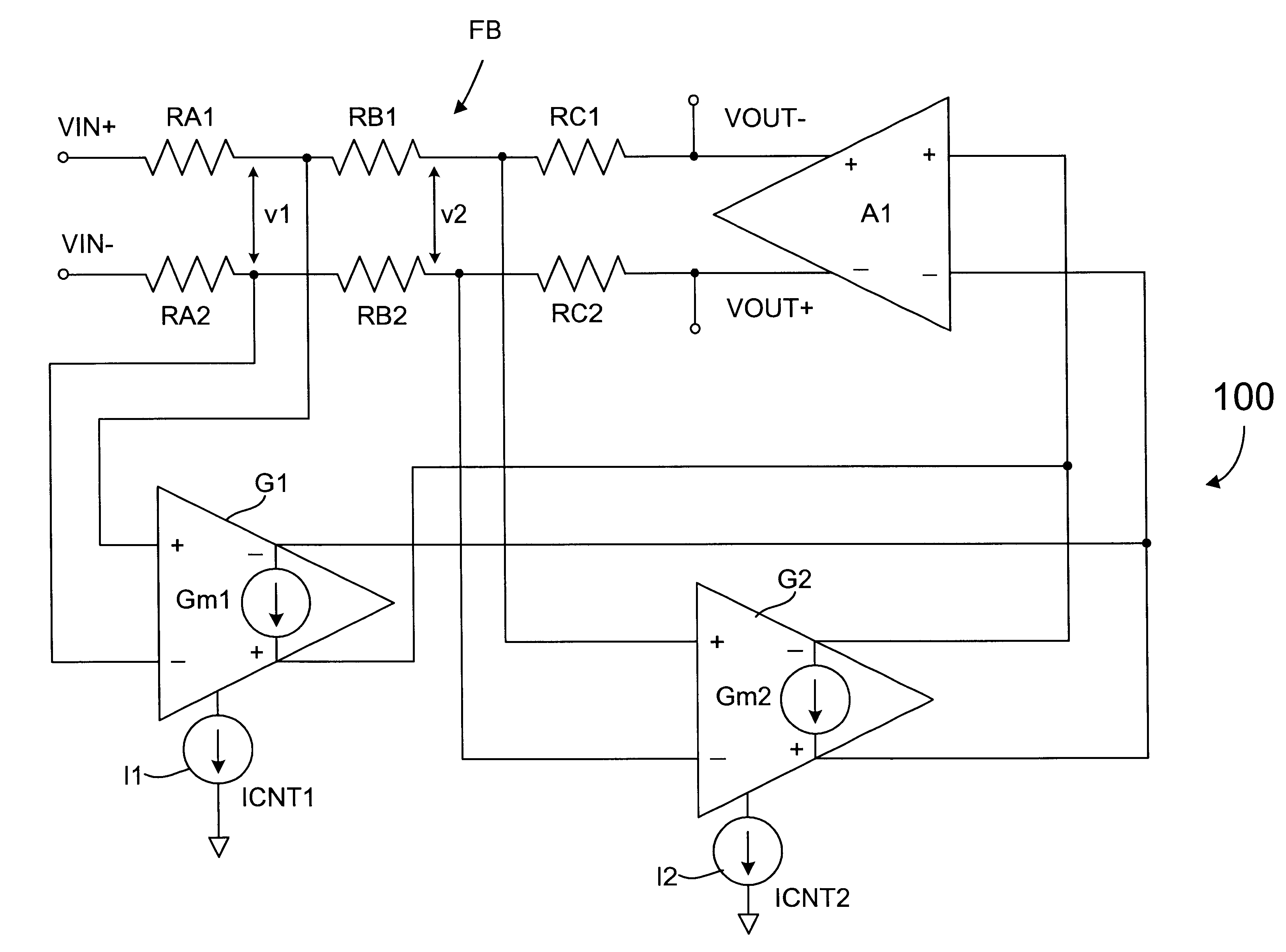
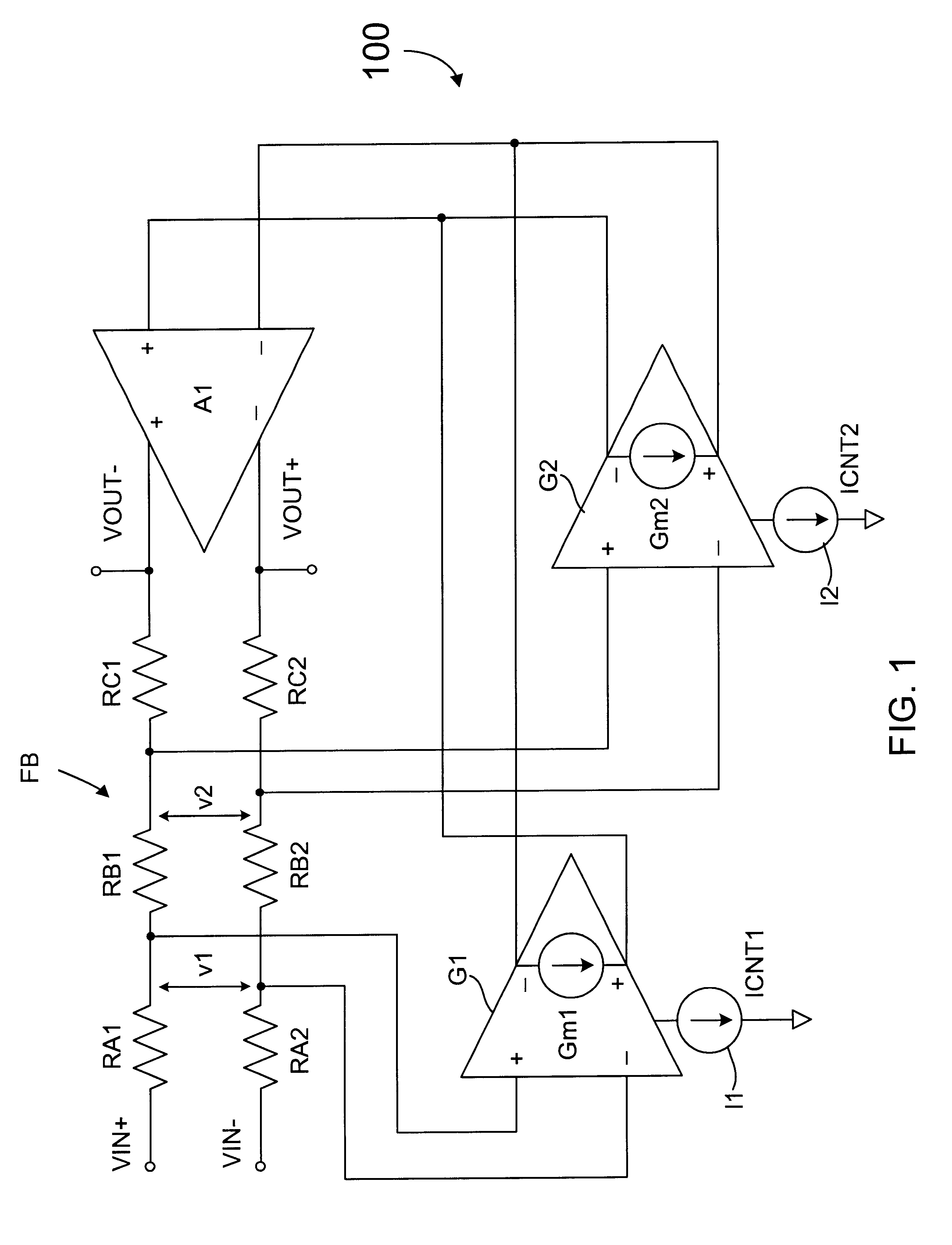
FIG. 1 is a schematic diagram of an exemplary AGC circuit 100 according to an embodiment of the present invention which exhibits high linearity and monotonically correlated offset voltage. The AGC circuit 100 includes six feedback resistors RA1, RA2, RB1, RB2, RC1 and RC2, a pair of transconductance amplifiers G1 and G2, a pair of control current sources I1 and I2, and a high gain transimpedance stage amplifier A1. The transconductance amplifiers G1 and G2 have transconductances Gm1 and Gm2, respectively. The control current sources I1 and I2 sink control currents ICNT1 and ICNT2, respectively. The AGC circuit 100 receives a differential input voltage VIN with positive and negative polarity signals VIN+ and VIN-, where VIN=(VIN+)-(VIN-). The AGC amplifier 201 provides a differential output voltage VOUT with positive and negative polarity signals VOUT+ and VOUT-, where VOUT=(VOUT+)-(VOUT-).

The input signals VIN+, VIN- are provided to respective ends of the two resistors RA1 and RA2. ...


PUM


Abstract

An automatic gain control (AGC) circuit including a high gain amplifier, a feedback network and two transconductance amplifiers. The feedback network has a first end that receives an input signal of the AGC circuit, a second end coupled to the output of the high gain amplifier and two intermediate nodes. Each transconductance amplifier has an input coupled to a respective intermediate node of the feedback network and an output coupled to the input of the high gain amplifier. The transconductance amplifiers collectively control a position of a virtual ground within the feedback network to control gain of the AGC circuit. The transconductance amplifiers each include an attenuator and a transconductance stage coupled between the feedback network and the high gain amplifier and are configured to operate linearly across a relatively wide input voltage range. The input offset voltage of the AGC circuit varies monotonically with gain of the AGC circuit.

Description

FIELD OAF THE INVENTIONThe present invention relates to an automatic gain control (ACG) circuit, and more particularly to an AGC circuit with high linearity and monotonically correlated offset voltage.DESCRIPTION OF RELATED ARTAutomatic Gain Control (AGC) circuits are used in many communication and signal processing applications. For example, in the receiver of a wired or wireless communication link, the intended signal to be processed may be a short distance away and therefore relatively strong while another signal may be a long distance away and much weaker. The receiver must process both the strong signals and the weak signals which implies a variable gain function. High gain is used to detect and amplify weak signals and low gain and / or attenuation is used to process strong signals.In certain architectures, such as a zero intermediate frequency (ZIF) radio architecture and the like, the AGC function requires a relatively large maximum voltage gain and wide total gain range capab...

Claims


Application Information

Patent Timeline
Patent Type & Authority Patents(United States)
IPC IPC(8): H03F3/45H03F1/32H03G3/30H03G3/20
CPCH03F1/3211H03F3/45085H03G3/3042H03F3/45973H03F3/456H03F2203/45574
Inventor PRENTICE, JOHN S.LANDY, PATRICK J.
Owner INTELLECTUAL VENTURES I LLC
Why Eureka
Try Eureka