Packaging types of light-emitting diode

a technology of light-emitting diodes and packaging types, which is applied in the association of printed circuit non-printed electric components, electrical apparatus construction details, and incorporation of printed electric components, etc., and can solve the problems of high power consumption, poor heat generation, and even worse current surface mount devices

Inactive Publication Date: 2003-05-13
SOLIDLITE CORP
View PDF1 Cites 92 Cited by
  • Summary
  • Abstract
  • Description
  • Claims
  • Application Information

AI Technical Summary

Benefits of technology

To avoid these things from happening and causing quality problems with LED reliability, the present invention specially emphasizes the use of high-temperature solder at about 250.degree. C.-500.degree. C., most preferably 350.degree. C. Of course, most soldering material is composed of Sn / Pb alloys. If the groove surface is plated with highly reflective materials like Ag or Au, the performance of groove reflector will be affected because Sn easily forms alloys with Au and Ag. Therefore, in the present invention an isolating layer of Cr or other layers that are not easy to form low-temperature alloys with solder material is plated prior to plating gold or silver film. Thus, the adverse effect can be avoided when the SMD LED connected with other printed circuit board in the present technology passes through the solder furnace and are subject to high temperature.

Problems solved by technology

Therefore, its power consumption is large, and heat generated is large as well.
In terms of heat dissipation in LED package, current surface mount device (SMD) is one of the worst, even worse than Lamp LED.
Large current can not be sustained.
The main reason for this is that effective heat conductance can not be achieved due to the poor heat dissipation of packaging resin and substrate itself.
Because the bottom inside the concave cup reflecting base made on printed circuit board through drilling holes is in curved shape (cause by drilling holes), the connection for die bonding of LED chips is poor and unstable.
If the groove surface is plated with highly reflective materials like Ag or Au, the performance of groove reflector will be affected because Sn easily forms alloys with Au and Ag.

Method used


Image

  • Packaging types of light-emitting diode
  • Packaging types of light-emitting diode
  • Packaging types of light-emitting diode

Examples


first embodiment

The

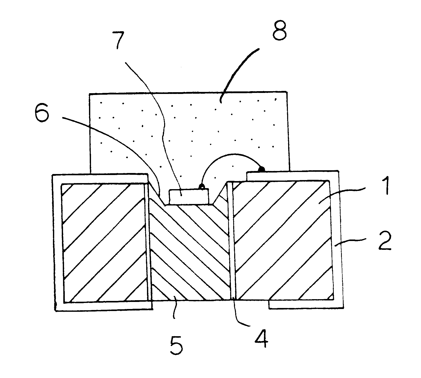
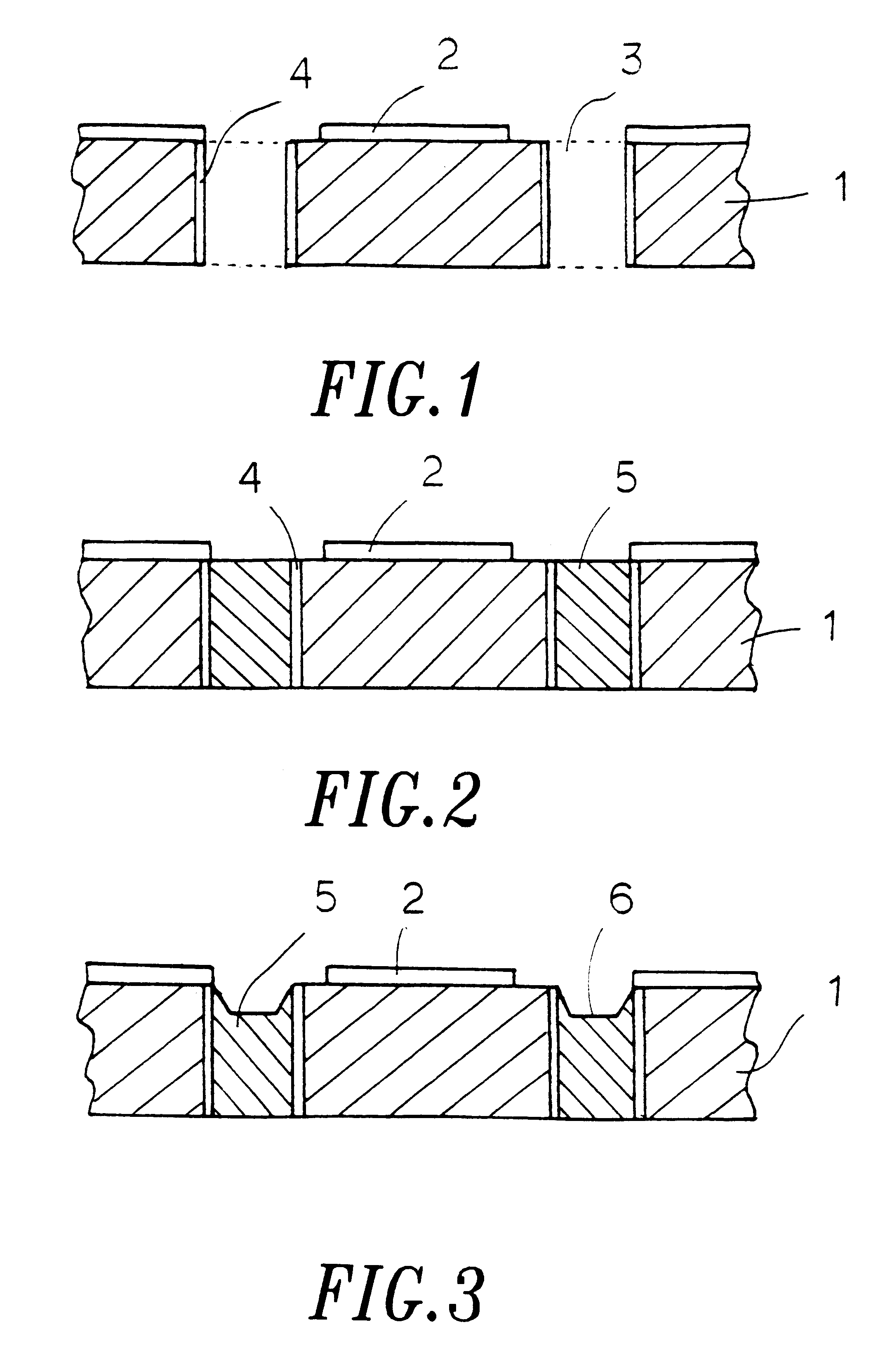
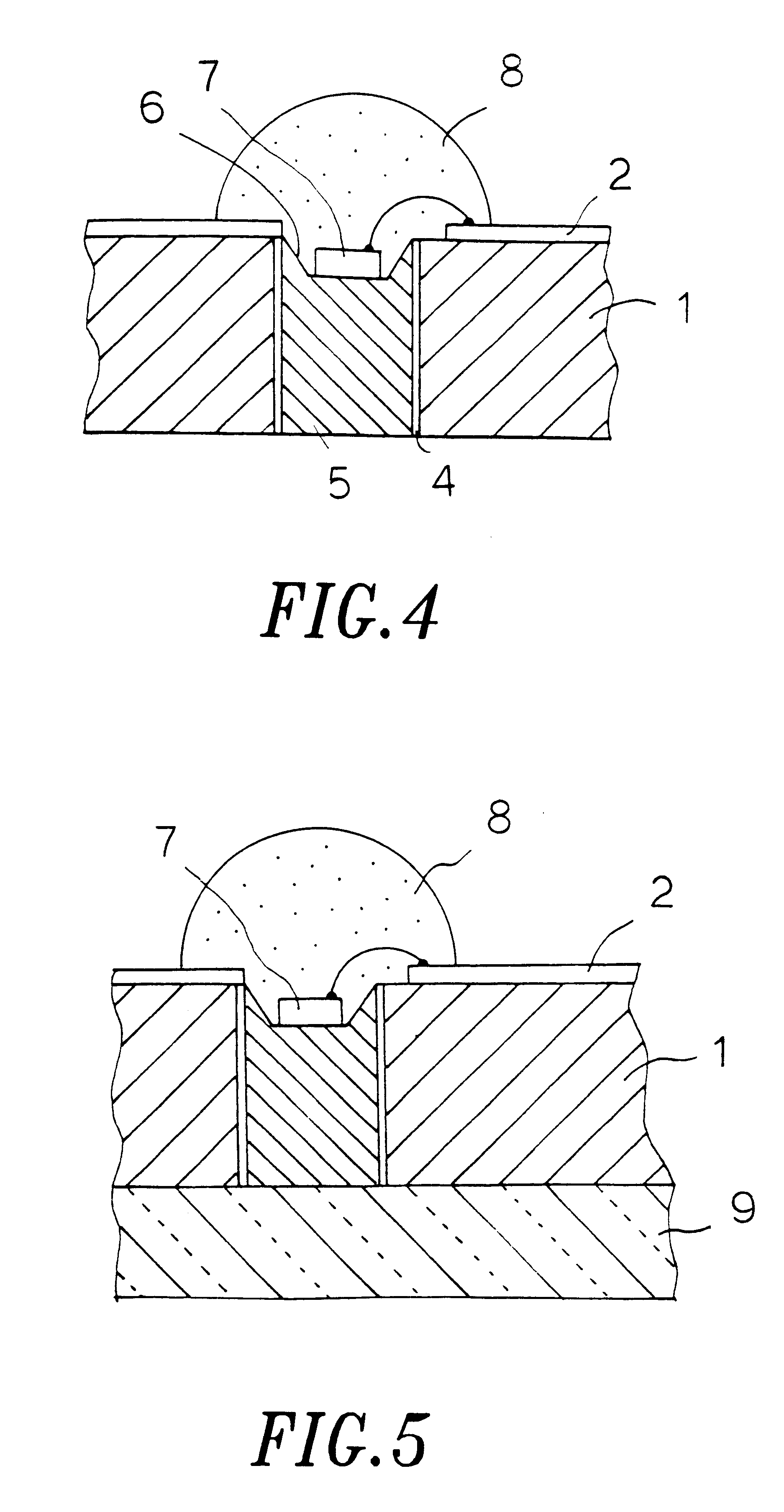
Please refer to FIG. 1, which illustrates the printed circuit board for the LED package in the present invention, wherein the packaging process includes producing electrode 2 on the surface of the printed circuit board substrate 1; forming through holes 3 by drilling at predetermined positions of the printed circuit board that LED chips are placed; plating the through holes on the printed circuit board to form through-hole plated metal layer 4; passing the printed circuit board through solder furnace to fill all through holes with solder to form soldering point 5 (as shown in FIG. 2); on the surface of soldering point 5, using molds to form a small groove that is plated on surface a metal layer or material (for example, Cr) that does not form low-temperature alloys with solder; plating a reflective layer of material like gold or silver; bonding LED chips to groove 6 and bonding wire; final filling with encapsulation resin 8 (as shown in FIG. 4) to form the finished product of LED...

second embodiment

The

Please refer to FIG. 8, which illustrates the printed circuit board substrate 1 of the second embodiment for the LED package in the present invention (the same as the substrate in the first embodiment), wherein the packaging process includes forming the positive and the negative electrode surfaces at electrode 2 on the substrate surface; directing the electrode to the bottom; forming a metal bump by plating a metal layer of mainly copper material on the electrode surface with placement of LED chips and wire bonding in advance; forming a smaller bump called electrode of metal bump 10 on a larger bump called electrode base of metal bump 11; using molds to make the bump to form a small groove 6 that has the same function as the small groove 6 in the first embodiment, both being used to place LED chips for die bonding and light reflection; plating highly reflective material like gold or silver on electrode base of metal bump 11 containing groove 6 and electrode of metal bump 10 to en...


PUM


Abstract

A LED packaging process is to place LED chips at predetermined positions on the printed circuit board substrate, followed by drilling holes to penetrate the substrate, followed by passing the printed circuit board through the solder furnace to completely fill the through-hole position with solder points, followed by using molds to make the soldering points into a groove reflector, followed by placing LED chips in the groove reflector, followed by wire bonding and using encapsulation resin for packaging to form SMD LED with reflectors. In the present invention, the filling with metal conductor in electrode through holes on the printed circuit board to form the groove reflector can enhance the heat dissipation of LED and the brightness of LED, which has the advantageous effects that traditional SMD LED can not have.

Description

1. Field of the InventionThe packaging of light-emitting diode (LED) basically has two types. One is LAMP type, which uses liquid resin for encapsulation. The present invention mainly uses the packaging process for SMD LED and also includes the new packaging technology of LED Chip on Board (COB).2. Description of the Prior ArtThe consideration of heat dissipation in LED package is very important, especially in the newest lighting application of white light LED, which no longer uses 15 mA or 20 mA as standard, but above 50 mA, even up to 100 mA (more brightness). Therefore, its power consumption is large, and heat generated is large as well. Hence, the heat dissipation ability should be enhanced. Hewlett Packard has developed a type of LED (called Super Flux LEDs by HP in model number HPWA-MHOO etc.) with special packaging structure (commonly called Perona fish), designed for good heat dissipation and can withstand up to 70 MA current (20 MA for traditional package). At present, LED ...

Claims


Application Information

Patent Timeline
Patent Type & Authority Patents(United States)
IPC IPC(8): H01L33/00H01L33/46H01L33/48H01L33/62
CPCH01L33/486H01L33/62H01L33/46H01L2224/48091H01L2924/12041H01L2924/01079H01L2924/01078H01L2924/00014
Inventor CHEN, HSING
Owner SOLIDLITE CORP
Why Eureka
Try Eureka