Active matrix liquid crystal display device having electrostatic shielding layer between data lines

a liquid crystal display device and active matrix technology, applied in static indicating devices, optics, instruments, etc., can solve problems such as block noise, uneven lines, and change in luminance, and avoid the effect of block nois

Inactive Publication Date: 2003-06-17
VISTA PEAK VENTURES LLC
View PDF8 Cites 35 Cited by
  • Summary
  • Abstract
  • Description
  • Claims
  • Application Information

AI Technical Summary

Problems solved by technology

However, in such block-at-a-time addressing, in the block boundary-portion of the adjacent data lines of the liquid crystal matrix, a luminance change occurs because of noise (block noise) generated during switching in the analog switching array of the data driver circuit, which results in the appearance of uneven lines.
This situation causes the foregoing problem of block noise.
Another problem inherent in the conventional active matrix liquid crystal display device is the long wiring distance between each driver circuit and the pixel matrix. FIG. 15 schematically shows a structure of the conventional active matrix liquid crystal display device.
If the driver circuits are provided inside the sealing region, then voltages supplied to the driver circuits subject liquid crystal molecules to electrolysis, generate impurity ions, and cause deterioration of display images.
Thus, electrostatic coupling capacitance between the data lines is increased and, during block-at-a-time addressing, noise is generated following the voltage fluctuation of the other data lines due to the electrostatic coupling capacitance, resulting in the problem of image quality degradation.
However, the installation of new metal layers to shield the data lines increases the number of manufacturing steps, and results in a complex device structure.
The irradiation of a strong light to a pixel thin-film transistor (TFT) results in problems including a reduction in contrast caused by a light leaking current, a generation of vertical crosstalk, and so on.

Method used


Image

  • Active matrix liquid crystal display device having electrostatic shielding layer between data lines
  • Active matrix liquid crystal display device having electrostatic shielding layer between data lines
  • Active matrix liquid crystal display device having electrostatic shielding layer between data lines

Examples


first embodiment

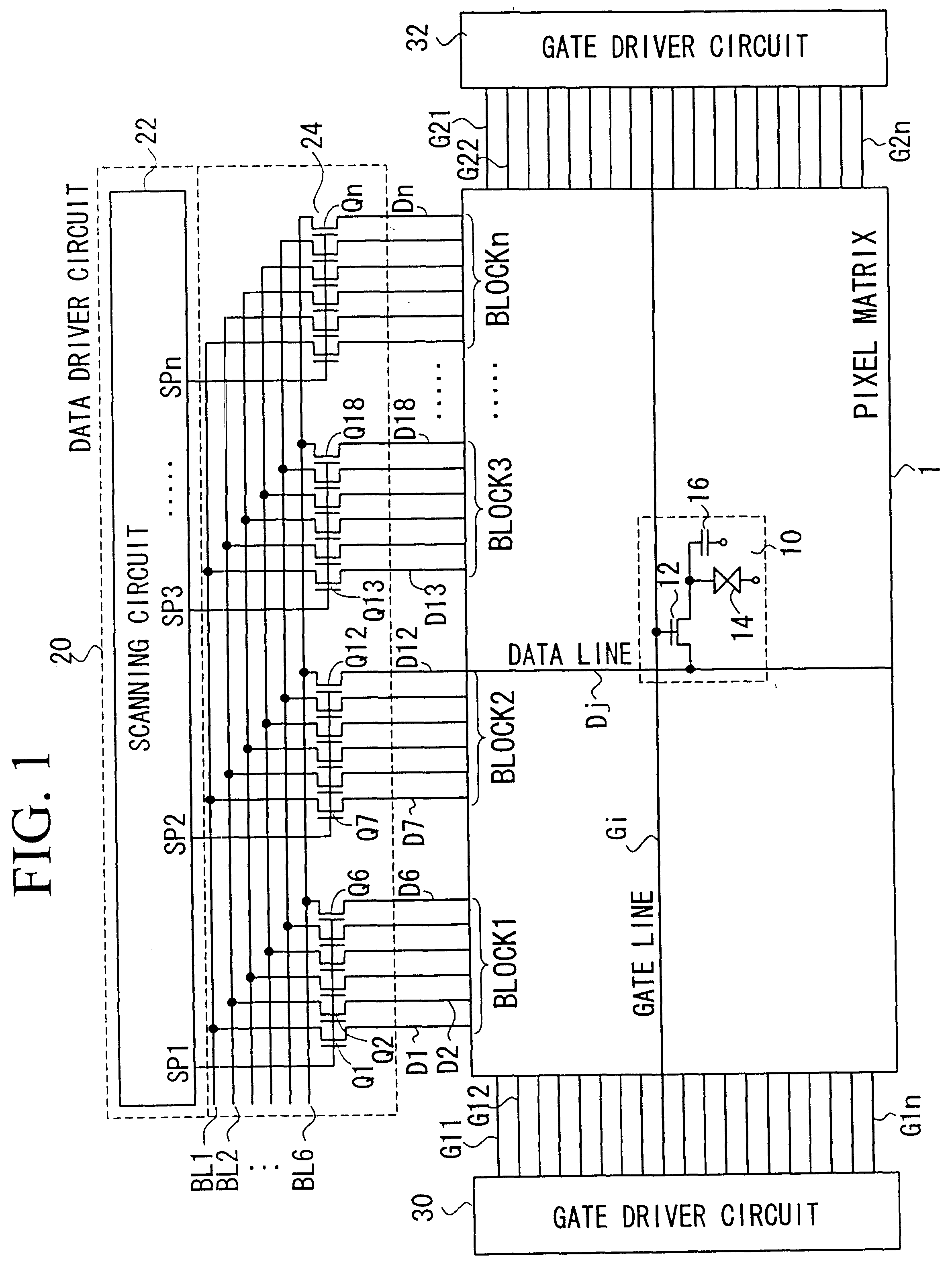
Next, detailed description will be made for the preferred embodiments of the present invention with reference to the accompanying drawings. FIG. 1 shows the circuitry of an active matrix liquid crystal display device according to the present invention. In the drawing, the active matrix liquid crystal display device comprises: a pixel matrix 1 composed of pixels that have pixel transistors, liquid crystal capacitance and storage capacitance, which are disposed at respective intersections between data lines D1 to Dn and gate lines G11 to G1n and G21 to G2n arranged longitudinally and latitudinally, respectively; a data driver circuit 20 for driving the data lines D1 to Dn; and gate driver circuits 30 and 32 for driving the gate lines G11 to G1n and G21 to G2n.

Regarding each pixel, e.g., a pixel 10 formed at an intersection between the data line Dj and the gate line Gi in FIG. 1, the pixel is composed of a pixel thin-film transistor (TFT) 12 having a gate connected to the gate line Gi ...

second embodiment

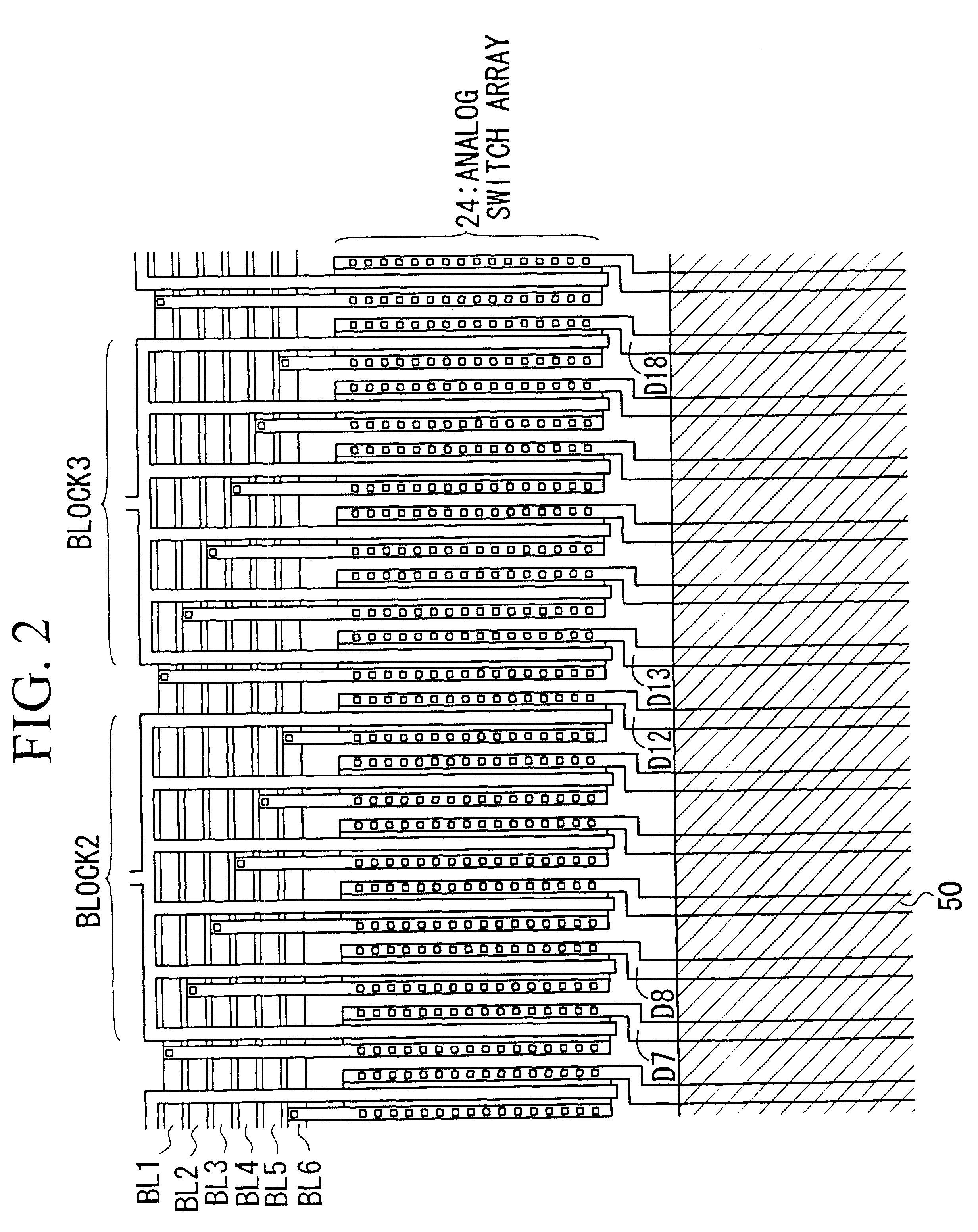
Next, a description will be made of an active matrix liquid crystal display device according to the present invention. Except for the shielding structure of the data lines, the circuitry of the active matrix liquid crystal display device of this embodiment is similar to that shown in FIG. 2, and thus description of similar portions will be omitted. Portions of the circuitry will be described by referring to FIG. 1 when necessary. FIG. 4 is a layout view showing wiring from the analog switch array 24 of the data driver circuit 20 to the pixel matrix 1.

FIG. 4 shows a shielding structure of the second embodiment of the present invention regarding the portions of the blocks 2 and 3 of the data lines in FIG. 1. In the drawing, a center portion indicates an analog switch array 24 of the data driver circuit 20. In this portion, switch transistors Q7 to Q12 and Q13 to Q18 are formed to perform block-at-a-time addressing for the data lines D7 to D12 (Block2) and D13 to D18 (Block3).

The data ...

third embodiment

Next, description will be made for an active matrix liquid crystal display device according to the present invention. Except the shielding structure of the data lines, the circuitry of the active matrix liquid crystal display device of this embodiment is the same as that shown in FIG. 1, and thus description of similar portions will be omitted. Description of the layout of wiring from the analog switch array 24 of the data driver circuit 20 to the pixel matrix will also be omitted, as it is similar to that shown in FIG. 4.

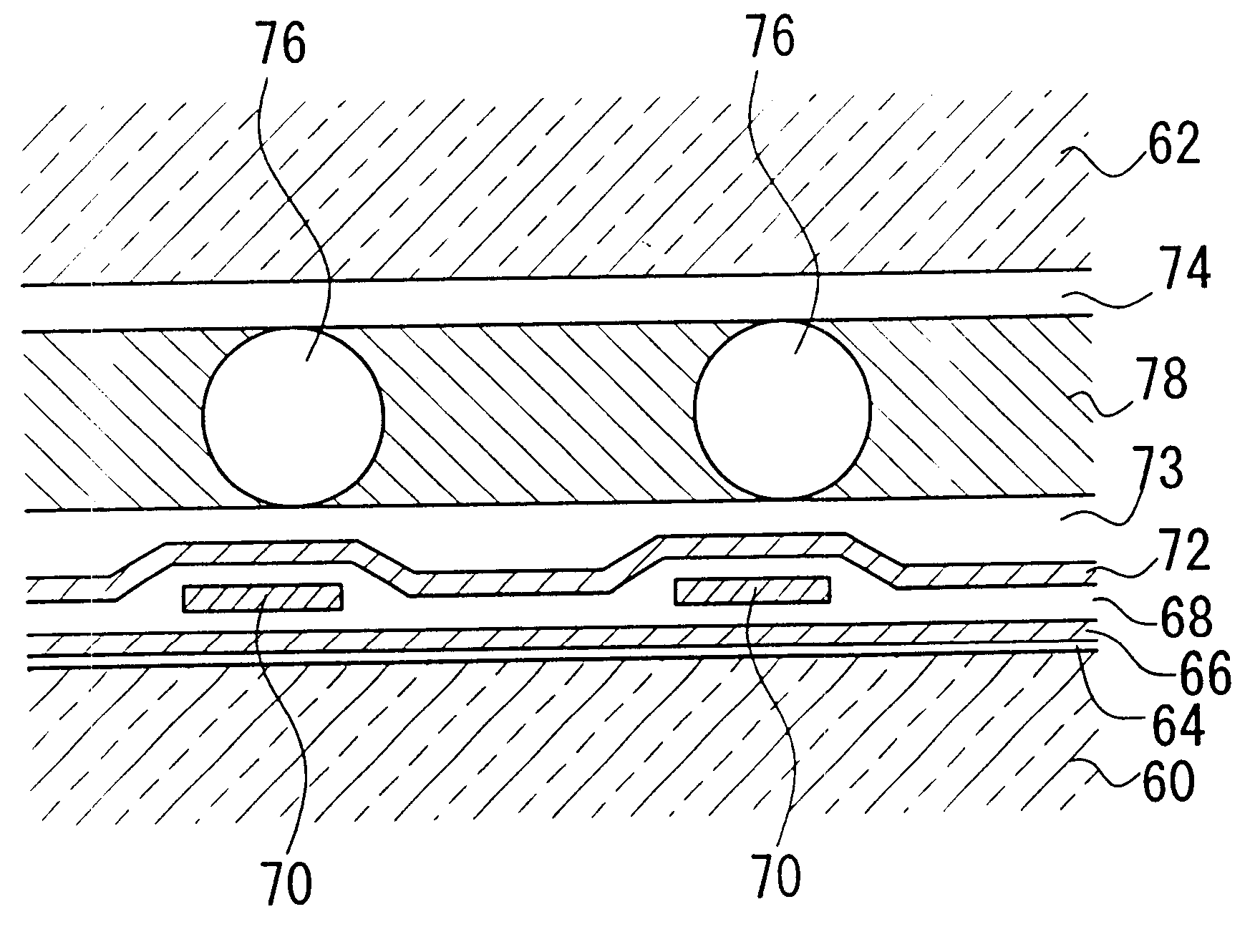
FIG. 6 shows a shielding structure of data lines of the active matrix liquid crystal display device of the third embodiment, i.e., a sectional structure of the sealing region cut in a direction orthogonal to the data line. In this case, as can be understood from FIG. 6, unlike the shielding structure of the data lines of FIG. 5, shield wiring 70A by the metal layer having the same metal as that of the data lines 70 is provided between the data lines 70 so as not to...


PUM

PropertyMeasurementUnit
capacitanceaaaaaaaaaa
storage capacitanceaaaaaaaaaa
electrostatic coupling capacitanceaaaaaaaaaa

Abstract

Disclosed is an active matrix liquid crystal display device, comprising: a pixel matrix; a data driver circuit for driving data lines; and gate driver circuits for driving gate lines. These constituting elements are all manufactured on the same substrate, and the data driver circuit and the gate driver circuits are formed outside a sealing region located outside the pixel matrix. In this case, all data lines formed between the data driver circuit and the pixel matrix are substantially covered by at least one metal layer which is composed of a metal different from that of the data lines, wherein the metal layer is adapted to perform both light shielding and reduction of electrostatic coupling capacitance between the data lines. Thus, it is possible to improve image quality by reducing noise generated following voltage fluctuation between data lines without providing any new metal layers for shielding.

Description

1. Field of the InventionThe present invention relates to an active matrix liquid crystal display device, and more particularly to a wiring structure of the active matrix liquid crystal display device.This specification is based on Japanese Patent Application (Application No. Hei 11-189720), the content of which is incorporated herein by reference.2. Description of the Related ArtFIG. 12 shows an example of the circuitry for a conventional active matrix liquid crystal display device. In the drawing, the active matrix liquid crystal display device includes pixels disposed at respective intersections between data lines K1 to Kn and gate lines G1 to Gm, which are respectively arranged longitudinally and latitudinally, a data driver circuit 200 provided to drive the data lines, and a gate driver circuit 202 provided to drive the gate lines. For each pixel, e.g., pixel 210 formed at the intersection between the gate line Gi and the data line Kj, the pixel is composed of a pixel transisto...

Claims


Application Information

Patent Timeline
Patent Type & Authority Patents(United States)
IPC IPC(8): G02F1/13G02F1/1362G02F1/1345H01L29/786G02F1/133G02F1/1333G02F1/1335G02F1/136G02F1/1368
CPCG02F1/13454G02F1/1345G02F1/133
Inventor SEKINE, HIROYUKI
Owner VISTA PEAK VENTURES LLC
Why Eureka
Try Eureka